User Guide
- 9 -
Vertilon Corporation, 66 Tadmuck Road, Westford, MA 01886 /Tel: (978) 692-7070 /Fax: (978) 692-7010 /www.vertilon.com
Specifications
(Vsupply = +5.0V, TA= +25C, unless otherwise noted)
Description Sym Min Typ Max Units Notes
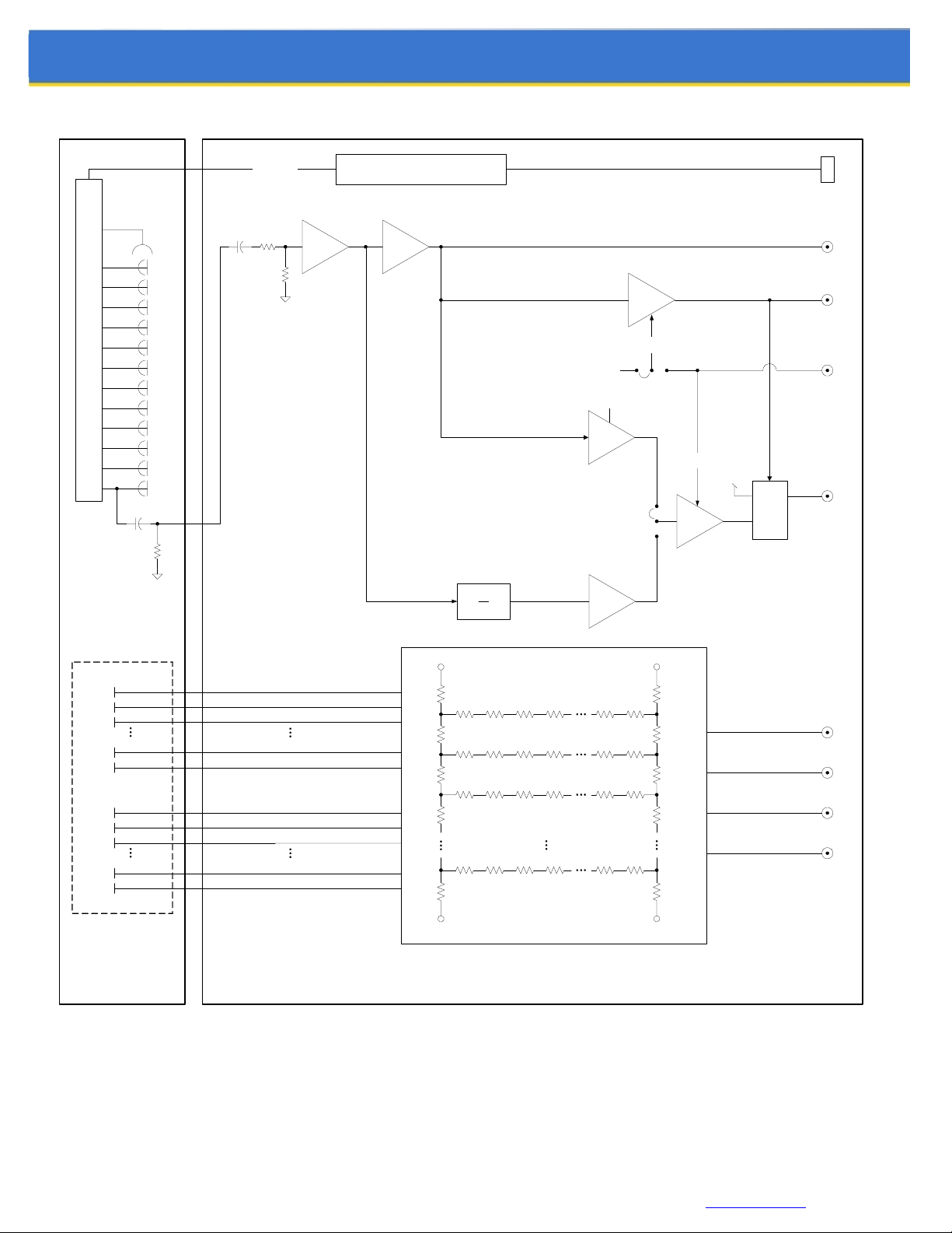
HIGH VOLTAGE
High Voltage Input Load Resistance 50 MMeasured at high voltage input connector, J1
ANODE CIRCUITS
Quantity P1 - P64 64
Input Bias Voltage +0.250 V Detector bias voltage supplied from PhotoniQ data
acquisition system
LAST DYNODE PREAMPLIFIER
Input Coupling Capacitance Cin 0.1 uF
Input Resistance Rin 50
Input Parallel Resistance Rp500
Amplifier #1 Gain A1 14.0 dB
Vin is a triangular pulse (18 nsec rise time, 30 nsec fall time)
applied to preamplifier input at DY12.
Amplifier #2 Inverting Gain A2 6 dB
Amplifier #2 Output Impedance 50 Measured at preamplifier output, J6
LEADING EDGE DISCRIMINATOR
Threshold Adjustment (External) Vth1 -100 0 mV Referenced to baseline level at comparator input. Controlled
using DSCR ADJ on J7 (+2.5V to +3.0V).
Threshold Adjustment (Internal) Vth1 -50 0 mV Referenced to baseline level at comparator input. Controlled
using potentiometer VR1.
Threshold to Output Delay (Vin=30mV) td1 5 nsec
Output on connector, J8.
Vin is a triangular pulse (18 nsec rise time, 30 nsec fall time)
applied to preamplifier input at DY12. Threshold (Vth1) set to
15mV below the baseline.
Time Walk (Vin: 3mV to 30mV) -13 nsec
Time Walk (Vin: 30mV to 150mV) -3.0 nsec
Jitter (Vin: 10mV) 1 nsec
ZERO SLOPE DISCRIMINATOR
Differentiator First-Order Time Constant 3.3 nsec
Amplifier #4 Inverting Gain A4 10.4 dB
Threshold Adjustment Vth3 0 +100 mV Referenced to baseline level at comparator input. Controlled
using DSCR ADJ on J7 (+2.5V to +2.0V).
Threshold to Output Delay (Vin=30mV) td3 7 nsec
Output on connector, J9.
Vin is a triangular pulse (18 nsec rise time, 30 nsec fall time)
applied to preamplifier input at DY12. Threshold (Vth3) set to
5mV above the baseline.
Time Walk (Vin: 20mV to 150mV) -3.0 nsec
Jitter (Vin: 100mV) 500 psec