Page 8of62
3.4Protection andFiltering
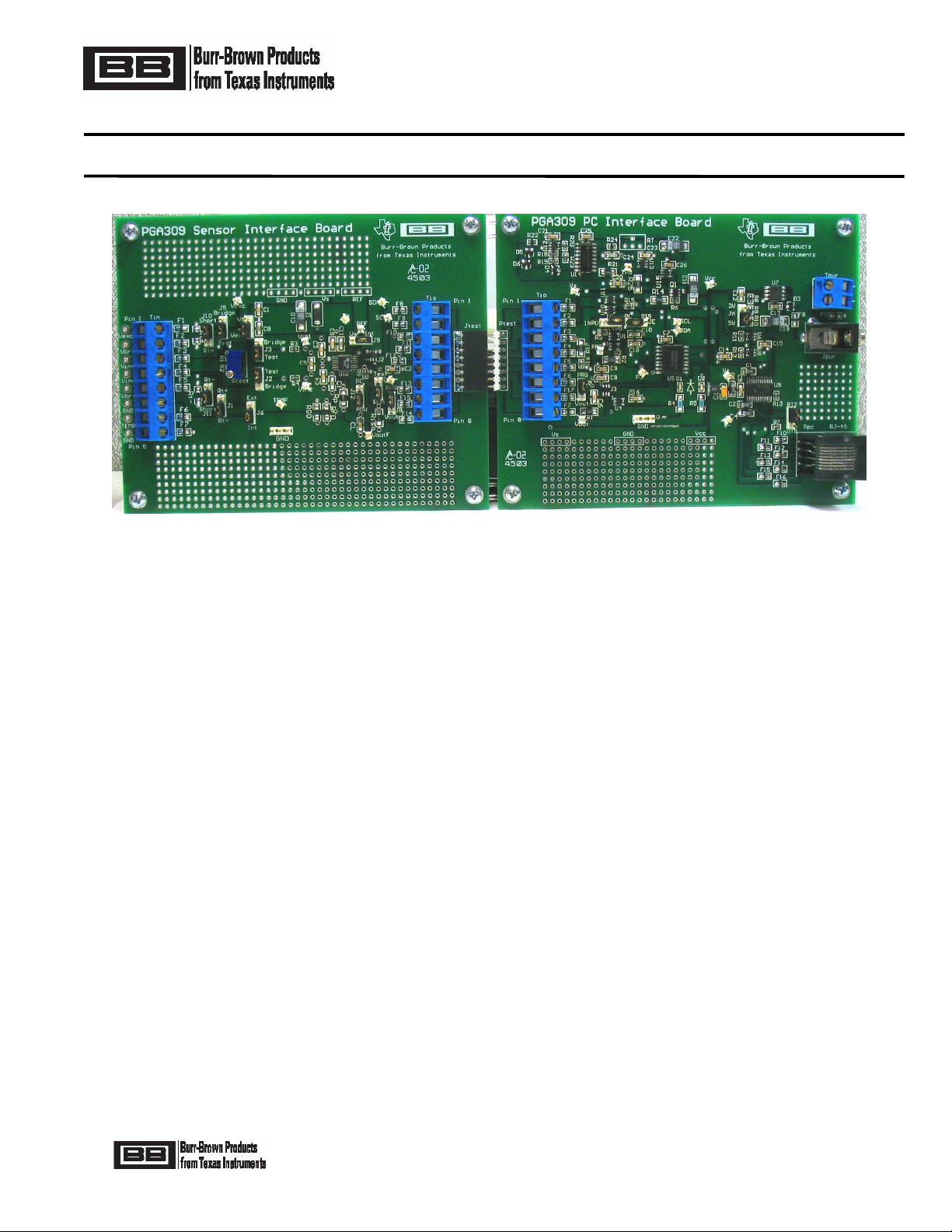
The PGA309 SensorInterfaceBoardisconfigured withcomponentstopreventmis-wiremishaps. If poweris
provided fromthe PGA309 PCInterfaceBoard,D1,isadequatetoprotectfromovervoltagesand reverse
polarityconnections. CL isastandardEMI/RFIcapacitordesign withRisoand Rp providing up to16V
overvoltage on VoutF.Input commonmode plusdifferential noisefiltering isprovided byC3,C4, C5and R3,
R4.
3.5TestPointsand MiscellaneousBreadboard Area
ThereareseveralTestPoints,including a3-position oneforGND, provided foreaseofmeasuring analog
signals. Alsoprovided arereserved areaswithplated-through, standard-spacing, 0.1”holesformiscellaneous
proof-of-concept breadboarding asdesired foragiven application.
4.0 PGA309 PCInterface BoardOverview –Part1
(RefertoPGA309 PCInterfaceBoardSchematic,Sheet 1of 2)
4.1Input/Output
The connectionsfromthe PGA309 PCInterfaceBoardtothe PGA309 SensorInterfaceBoardareprovided
through Tio, an 8-position screwterminal strip. Thisconnectorprovideseaseofconnectionstowiresforthe
required selected signalswhen placing the PGA309 SensorInterfaceBoardinside atemperaturechamberfor
PGA309 +Sensorcalibration.Inparallel withTioisPtest whichprovidesameansfordirectplug-inconnection
tothe PGA309 SensorInterfaceBoard.Thisisuseful forinitial checkoutofthe PGA309EVM system.Ppcis
an 8-position RJ45 jack forconnection through the PGA309EVM PCcabletoatest computer’sRS-232 serial
port. RS-232 compatiblesignalsaregenerated through U9. Powerforthe PGA309 PCInterfaceBoardis
provided through eitherJpwrorTpwr.Jpwristobe used whenan ACWallAdapter(120VacRMS, 60Hzin;
6Vdc, 200mAout)isavailable–USA ShipmentsOnly.Otherapplicationswillusea6Vdc(6Vdc-9Vdc) lab
supplyand the screwterminalinputson Tpwr. U7 providesaregulated powersourceofeither3Vor5V,
selectablethrough JA.D3 providesprotection frominadvertentreversepolarityconnectionson JpwrorTpwr.
4.2PortExpander Configuration Control
U5 isan 8-bit serial port expanderPCF8574Awhichallowsusercontroloverthe configuration of the PGA309
PCInterfaceBoard.D1 and D2 arecontrolled bythe BoardControlSoftwareand areused asdiagnostic
LEDs. Q1,alsocontrolled through U5, providesamechanismtoturnpoweron and off tothe PGA309 Sensor
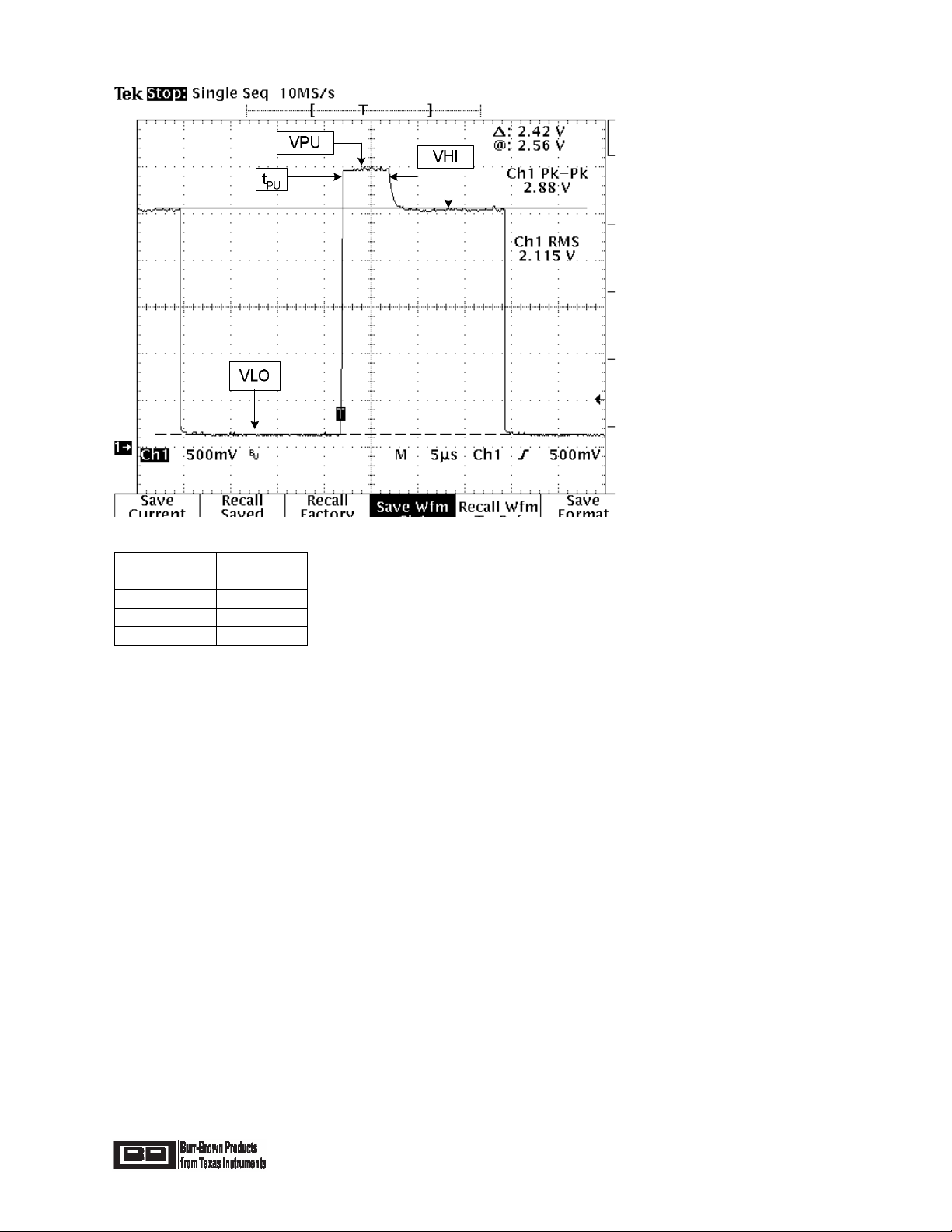
InterfaceBoardbytheBoardControl Software. Thisiskeywhen PRG isconnected toVout onthe PGA309
sinceVoutisset tohigh impedanceon power-up for25mstoallowforOne-Wirecommunication.Anunused
port, P3, pin7isavailableforcustomerusewithcontrolprovided intheBoardControlSoftware. The One-
Wirepull-up resistor, R3can be disabled through U5 toremoveloading fromthe PGA309 Vout pinforan
accuratereadout through the ADS1100, U3.U5 alsocontrolsthe zerocalibration ofthe ADS1100.TheTwo-
Wireinterfacecan be isolated fromthe PGA309 SensorInterfaceBoardbysoftwarethrough U5 controlof U10
and U11 oralsobyhardwarejumperprogramming.
4.3One-Wire DigitalInterface
OnthisDesigner’sKit the One-Wiredigitalinterfaceisthe preferred mode ofcommunication withPGA309.It
isprovided through the conversion ofRS-232 UART signalsfromU9 intoopen drainoutputthrough U2.The
resistivepull-up forthe One-Wireinterfaceisenabled ordisabled through U1.TheOne-Wirepull-up can be
disabled foran accuratePGA309 Voutreading withoutthe extraloading due toR3.JCprovidesaselection
forthe One-Wireactivepull-up (1PU)ornoOne-Wireactivepull-up (1NPU).Thisfeatureisdescribed indetail
inSection 5.1.JumperJB providesamechanismforcommunication through Vout when PRGistiedtoVout
on the PGA309 fora3-terminal sensormoduleconfiguration.