1
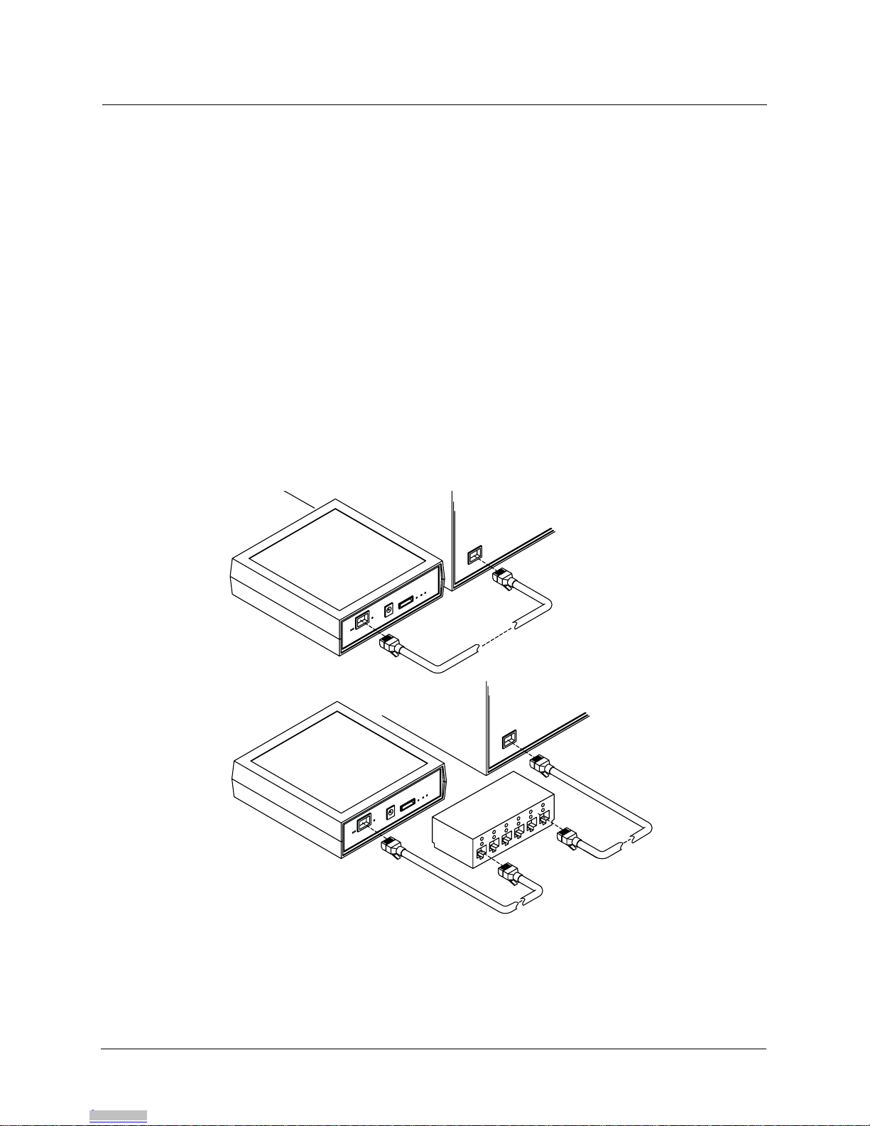
Figure QS-1 Connecting the computer.....................................................................................................................QS-iii
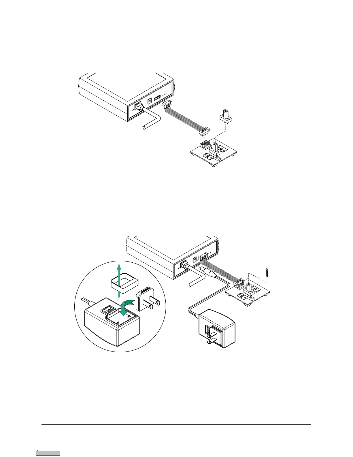
Figure QS-2 Connecting ribbon cable ......................................................................................................................QS-iv
Figure QS-3 Connecting power supply.....................................................................................................................QS-iv
Figure 1-1 ASEK System Configuration ...................................................................................................................... 1-3
Figure 2-1 ASEK software interface, Main page.......................................................................................................... 2-3
Figure 2-2 ASEK software interface, IP address setting page..................................................................................... 2-4
Figure 3-1 ASEK Main Board module, rear view......................................................................................................... 3-2
Figure 3-2 Direct connection options........................................................................................................................... 3-3
Figure 3-3 ASEK Power supply set............................................................................................................................. 3-4
Figure 3-4 Changing power supply prongs.................................................................................................................. 3-4
Figure 3-5 Linear device, output-pin programming PCB (PN 85-0329-101) layout..................................................... 3-6
Figure 3-6 Linear device, output-pin programming PCB (PN 85-0329-101) basic schematic..................................... 3-6
Figure 3-7 Layout of C2, CBLOW, socket on linear device (output pin programming) interface board......................... 3-7
Figure 3-8 Bipolar switch or latch device, supply-pin programming PCB (PN 85-0329-102) layout............................ 3-8
Figure 3-9 Bipolar switch or latch device, supply-pin programming PCB (PN 85-0329-102) basic schematic............ 3-8
Figure 3-10 Pre-designed DUT socket mounting ........................................................................................................ 3-9
Figure 3-11 Jumping unused GND terminals on the VCC programming PCB.......................................................... 3-10
Figure 3-12 ASEK Main Board ribbon cable header pin-out...................................................................................... 3-11
Figure 4-1 ASEK Interface, page for programming standard linear devices ............................................................... 4-3
Figure 4-2 ASEK Interface, page for programming A137x style linear devices........................................................... 4-5
Figure 4-3 ASEK page for switch/latch programming.................................................................................................. 4-7
Figure 4-4 ASEK Interface, opening page for the Desktop Utility downloads.............................................................. 4-9
Figure 4-5 Security confirmation box for the Desktop Utility download ..................................................................... 4-10
Figure 4-6 ASEK Desktop Utility interface................................................................................................................. 4-11
Figure 4-7 ASEK 136X Utility interface...................................................................................................................... 4-15
Figure 5-1 Board Calibration Utility page..................................................................................................................... 5-2
Figures
Downloaded from Arrow.com.Downloaded from Arrow.com.Downloaded from Arrow.com.Downloaded from Arrow.com.Downloaded from Arrow.com.Downloaded from Arrow.com.Downloaded from Arrow.com.