PulseBlasterDDS-I-300
Table of Contents
Table of Contents ................................................................................................................................... 3
I. Introduction ......................................................................................................................................... 4
Product Overview ....................................................................................................................................................... 4
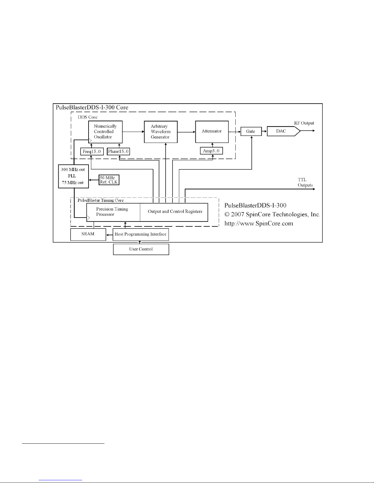
Board Architecture ...................................................................................................................................................... 4
Block Diagram ....................................................................................................................................................... 4
Product S ecifications ................................................................................................................................................ 6
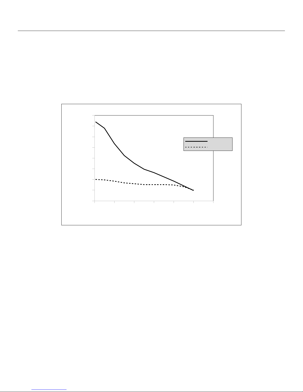
RF Out ut Level ........................................................................................................................................................... 7
II. Installation .......................................................................................................................................... 8
Installing the PulseBlasterDDS-I-300 ......................................................................................................................... 8
Testing the PulseBlasterDDS-I-300 ............................................................................................................................. 9
III. Using the PulseBlasterDDS-I-300 ................................................................................................. 11
Controlling the PulseBlasterDDS-I-300 with S inAPI .............................................................................................. 11
Frequency and Phase Registers ............................................................................................................................... 11
Sample Output ..................................................................................................................................................... 12
Sha e and Am litude Registers (AWG) ................................................................................................................... 14
Sample Output ..................................................................................................................................................... 14
Pulse Programs .......................................................................................................................................................... 16
Control lines ......................................................................................................................................................... 17
Triggering ................................................................................................................................................................... 18
Clock out ut on BNC0 ............................................................................................................................................... 18
Clock In ut Signal Standard ..................................................................................................................................... 19
IV. PCI Connection - Connecting to the PulseBlasterDDS-I-300-PCI boards ................................ 20
Connector Information .............................................................................................................................................. 20
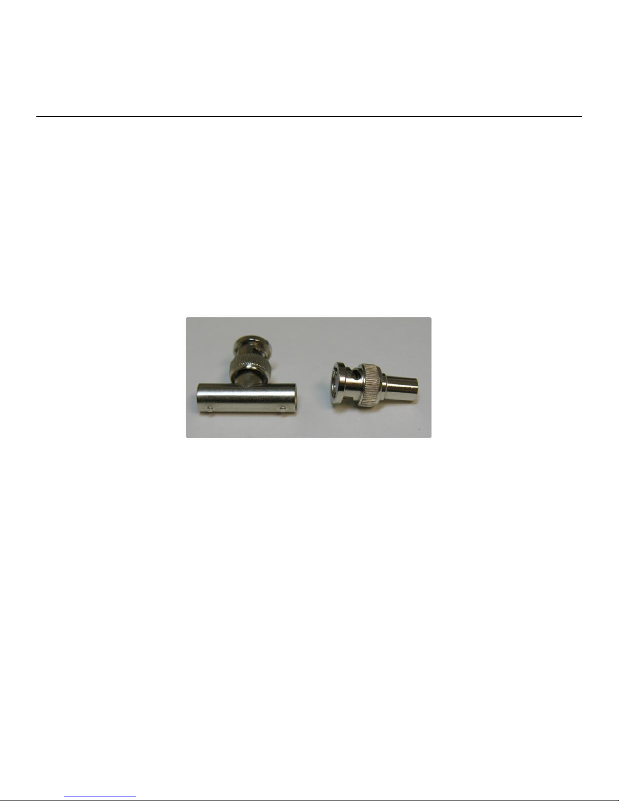
BNC Connectors .................................................................................................................................................. 20
Long IDC Hea ers ............................................................................................................................................... 20
HWTrig/Reset Hea er .......................................................................................................................................... 21
V. USB Connection - Connecting to the PulseBlasterDDS-I-300-USB boards .............................. 22
Power Requirements ................................................................................................................................................. 22
Power Connectors .................................................................................................................................................... 22
Digital Out ut Connectors ....................................................................................................................................... 23
Header JP302 ............................................................................................................................................................ 25
Connector Locations ................................................................................................................................................. 25
VI. External Frequency Modulation .................................................................................................. 26
Hea er JP302 (Frequency Select an HW Trigger/Reset) ................................................................................... 26
Important Notes: .................................................................................................................................................. 27
VII. PulseBlasterDDS-I-300 Interface for LabVIEW .......................................................................... 27
Overview of S inCore LabVIEW GUI Interface ........................................................................................................ 27
Related Products and Accessories ................................................................................................... 28
Contact Information ............................................................................................................................. 29
Document Information ........................................................................................................................ 29
http://www.spincore.com 3 2017-11-14