SiT8925B High Frequency, Automotive AEC-Q100 Oscillator
Programmable Drive Strength
The SiT8925 includes a programmable drive strength
feature to provide a simple, flexible tool to optimize the
clock rise/fall time for specific applications. Benefits from
the programmable drive strength feature are:
Improves system radiated electromagnetic interference
(EMI) by slowing down the clock rise/fall time.
Improves the downstream clock receiver’s (RX) jitter by
decreasing (speeding up) the clock rise/fall time.
Ability to drive large capacitive loads while maintaining
full swing with sharp edge rates.
For more detailed information about rise/fall time control
and drive strength selection, see the SiTime Application
Notes section.
EMI Reduction by Slowing Rise/Fall Time
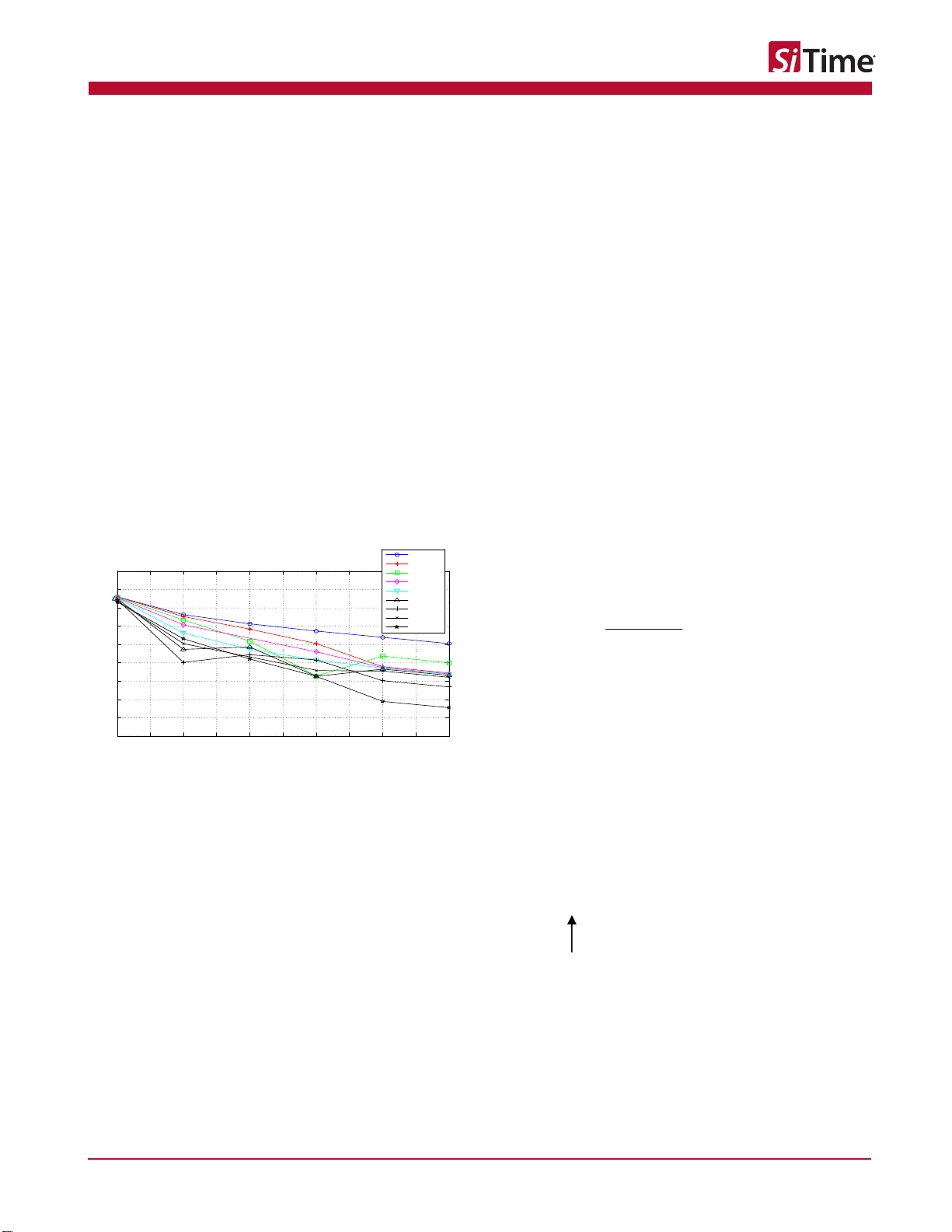
Figure 15 shows the harmonic power reduction as the
rise/fall times are increased (slowed down). The rise/fall
times are expressed as a ratio of the clock period. For the
ratio of 0.05, the signal is very close to a square wave.
For the ratio of 0.45, the rise/fall times are very close to
near-triangular waveform. These results, for example,
show that the 11th clock harmonic can be reduced by
35 dB if the rise/fall edge is increased from 5% of the
period to 45% of the period.
1 3 5 7 9 11
-80
-70
-60
-50
-40
-30
-20
-10
0
10
Harmonic number
Harmonic amplitude (dB)
trise=0.05
trise=0.1
trise=0.15
trise=0.2
trise=0.25
trise=0.3
trise=0.35
trise=0.4
trise=0.45
Figure 15. Harmonic EMI reduction as a Function
of Slower Rise/Fall Time
Jitter Reduction with Faster Rise/Fall Time
Power supply noise can be a source of jitter for the
downstream chipset. One way to reduce this jitter is to
speed up the rise/fall time of the input clock. Some
chipsets may also require faster rise/fall time in order to
reduce their sensitivity to this type of jitter. Refer to the
Rise/Fall Time Tables (Table 7 to Table 11) to determine
the proper drive strength.
High Output Load Capability
The rise/fall time of the input clock varies as a function of
the actual capacitive load the clock drives. At any given
drive strength, the rise/fall time becomes slower as the
output load increases. As an example, for a 3.3V
SiT8925 device with default drive strength setting, the
typical rise/fall time is 0.46 ns for 5 pF output load. The
typical rise/fall time slows down to 1 ns when the output
load increases to 15 pF. One can choose to speed up the
rise/fall time to 0.72 ns by then increasing the driven
strength setting on the SiT8925 to “F”.
The SiT8925 can support up to 30 pF in maximum
capacitive loads with up to 3 additional drive strength
settings. Refer to the Rise/Tall Time Tables (Table 7 to 11)
to determine the proper drive strength for the desired
combination of output load vs. rise/fall time.
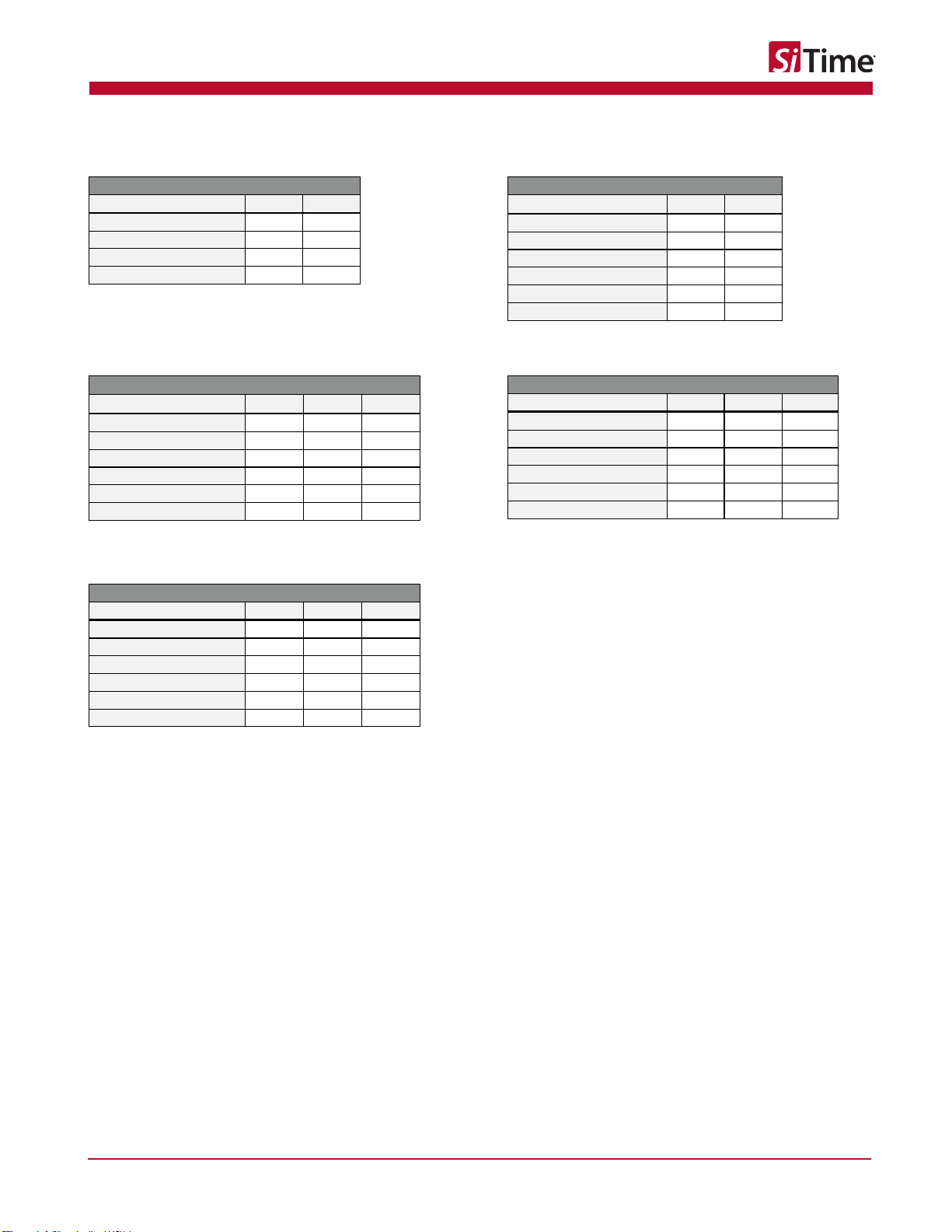
SiT8925 Drive Strength Selection
Tables 7 through 11 define the rise/fall time for a given
capacitive load and supply voltage.
1. Select the table that matches the SiT8925 nominal
supply voltage (1.8V, 2.5V, 2.8V, 3.0V, 3.3V)
2. Select the capacitive load column that matches the
application requirement (5 pF to 30 pF)
3. Under the capacitive load column, select the
desired rise/fall times.
4. The left-most column represents the part number
code for the corresponding drive strength.
5. Add the drive strength code to the part number for
ordering purposes.
Calculating Maximum Frequency
Based on the rise and fall time data given in Tables 7
through 11, the maximum frequency the oscillator can
operate with guaranteed full swing of the output voltage
over temperature as follows:
=1
5 x Trf_20/80
Max Frequency
where Trf_20/80 is the typical value for 20%-80% rise/fall
time.
Example 1
Calculate fMAX for the following condition:
Vdd = 3.3V (Table 11)
Capacitive Load: 30 pF
Desired Tr/f time = 1.46 ns
(rise/fall time part number code = U)
Part number for the above example:
SiT8925BAE12-18E-137.000000
Drive strength code is inserted here. Default setting is “-”