SEMCO Proprietary Information
The PHTS108 standard RF output frequency range covers L and S-Bands (1435.5-2394.5 MHz).
Modulation formats include PCM/FM, PM, BPSK, QPSK, IRIG 106-17 Tier I SOQPSK-TG and Tier II
Multi-h CPM. An embedded Bit Synchronizer, Frame Synchronizer and BERT that includes a Pseudo-
Random Code Generator is also provided.
The PHTS108 provides a phase-locked RF source and modulator with user-selectable, calibrated RF
signal outputs from 0 dBm to -100 dBm in 0.1 dB increments.
The PHTS108 can also be externally modulated with either a user-provided signal and test pattern,
or pre-recorded mission data using the simulator’s binary file playback feature.
Options include: C-Band RF Tuning (4400 to 5250 MHz); Dual RF Output and Fade/Phase feature for
dynamic diversity combiner testing; FM/FM Sub-Carrier and NTSC Video; and High power options
extending the PHTS108 output levels to +20 dBm, +30 dBm or +37 dBm.
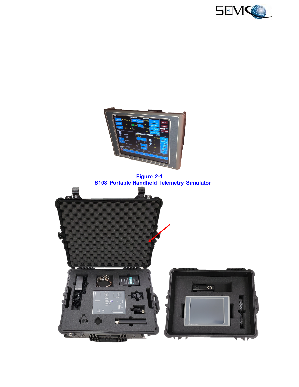
PHTS108 system set-up, control and status monitoring is provided by a 12” front panel Touch Screen
and remote (network) software via Ethernet.
2.2 Initial Hardware Set-up and Operation
The user should read this User’s Guide and become familiar and comfortable with the overall features,
options and configuration of the specific PHTS108 system that will be used. Table 2-2 lists and describes
the PHTS108 I/O. Figure 2-4 illustrates the PHTS108 I/O of standard configuration with respect to AC
and DC battery power, inputs, outputs and Touch Screen controls.
Figure 2-5 is the standard “D” connector cable harness assembly originally provided with the PHTS108.
Figure 2-6 is the current standard “D” connector cable harness assembly per the date of this manual
release that also supports the Dual RF Output and Dynamic Combiner Test Option.
Table 2-2
PHTS108 Simulator I/O
PHTS108 operates on 115/230 VAC, 50/60 Hz power via an adapter power cord
PHTS108 operates on 12 VDC battery power
Modulated RF “N” connector output from 0 dBm to -100 dBm
2 Modulated RF “N” connector outputs from 0 dBm to -100 dBm
Earlier Version External D
Connector Cable Assembly
J2 - Bit Sync Data In (BNC)
J3 - TTL Clock Out (BNC)
J4 - TTL Data Out (BNC)
J5 Pin 1 - RS422 External Modulation Data In +
J5 Pin 2 - RS422 External Modulation Clock In +
J5 Pin 5 - RS422 External Modulation Data In -
J5 Pin 6 - RS422 External Modulation Clock In -
Current Version External D
Connector Cable Assembly
Same J2, J3 and J4 BNC I/O as above
J5 Pin 1 - GND
J5 Pin 2 - Serial Data
J5 Pin 3 - Serial Latch
J5 Pin 4 - 3.3 VDC
J5 Pin 6 - GND
J5 Pin 7 - CH1 Fade
J5 Pin 8 - CH2 Fade
BNC Digital TTL Data Input to Bit Synchronizer
BNC Digital TTL Clock Input to Bit Synchronizer