Nordic Semiconductor nRF9160 Manuel utilisateur

nRF9160 DK Hardware
v1.1.0
User Guide
4418_1216 / 2022-04-19

Contents
Revision history.................................. iv
1Introduction................................... 6
2Kit content.................................... 7
3Operating modes................................ 8
3.1 Firmware development mode ........................... 8
3.1.1 Device programming ............................. 8
3.1.2 Virtual COM port ............................... 8
3.1.3 MSD .................................... 9
3.1.4 Reset .................................... 9
3.2 Performance measurement mode ......................... 10
3.2.1 USB detect ................................. 10
4Hardware description............................. 12
4.1 Hardware figures ................................ 12
4.2 Block diagram ................................. 12
4.3 Power supply ..................................13
4.3.1 nRF9160 supply ............................... 16
4.3.2 VDD supply rail ............................... 16
4.3.3 Other power domains ............................ 17
4.4 Antenna interfaces ............................... 17
4.5 GPS ...................................... 17
4.6 GPIO interfaces ................................. 18
4.7 nRF52840 ................................... 20
4.7.1 nRF9160 DK board control .......................... 20
4.7.2 Bluetooth/IEEE 802.15.4 network processor ................... 23
4.8 Buttons, slide switches, and LEDs ......................... 24
4.9 I/O expander .................................. 25
4.10 External memory ............................... 27
4.11 Debug input and trace options .......................... 27
4.12 Debug output ................................. 28
4.12.1 Connectors for programming external boards .................. 29
4.13 Signal routing switches ............................. 30
4.13.1 Interface MCU disconnect switches ...................... 31
4.13.2 Switches for UART interface ......................... 31
4.13.3 Switches for buttons and LEDs ........................ 32
4.13.4 Switches for nRF52840 interface ....................... 33
4.13.5 Switches for external memory ........................ 34
4.13.6 Switches for I/O expander .......................... 35
4.14 SIM and eSIM ................................. 35
4.15 Additional interfaces .............................. 36
4.16 SiP enable .................................. 37
4.17 Solder bridge configuration ........................... 37
5Measuring current............................... 39
5.1 Preparing the development kit for current measurements ............... 39
5.2 Using an oscilloscope for current profile measurement ................ 40
4418_1216 ii

5.3 Using a current meter for current measurement ................... 40
6RF measurements............................... 42
7Radiated performance of nRF9160 DK.................... 43
Glossary ..................................... 44
Recommended reading.............................. 47
Legal notices................................... 48
4418_1216 iii

Revision history
Date Description
2022-04-19 • Updated to match nRF9160 DK v1.1.0
• Editorial changes
2021-10-26 • Updated nRF9160 DK board control on page 20
• Editorial changes
November 2020 Updated to match nRF9160 DK v0.15.0 and nRF9160 DK v1.0.0
• Updated:
•Kit content on page 7
•Figure 7: nRF9160 DK block diagram on page 13
•Firmware development mode on page 8
•Performance measurement mode on page 10
•Hardware description on page 12
•GPS on page 17
•nRF9160 DK board control on page 20
• New:
•I/O expander on page 25
•External memory on page 27
•Switches for I/O expander on page 35
•Switches for external memory on page 34
July 2020 Updated document title
April 2020 Editorial changes
March 2020 • Updated Recommended reading on page 47
• Updated Debug output on page 28
• Added Connectors for programming external boards on page 29
October 2019 Updated to match nRF9160 DK v0.9.0
• Updated:
•Kit content on page 7
•Recommended reading on page 47
•Firmware development mode on page 8
•Performance measurement mode on page 10
•Block diagram on page 12
•Hardware figures on page 12
•Power supply on page 13
•Antenna interfaces on page 17
•GPS on page 17
•nRF9160 DK board control on page 20
•SIM and eSIM on page 35
•Additional interfaces on page 36
4418_1216 iv

Revision history
Date Description
•Solder bridge configuration on page 37
•Preparing the development kit for current measurements on page 39
• New:
•Interface MCU disconnect switches on page 31
•Switches for UART interface on page 31
•Switches for nRF52840 interface on page 33
• Removed:
• Getting started
July 2019 Updated:
•nRF9160 supply on page 16
March 2019 Updated to match nRF9160 DK v0.8.5:
•Kit content on page 7
•nRF9160 supply on page 16
•Antenna interfaces on page 17
•GPS on page 17
•nRF9160 DK board control on page 20
•Solder bridge configuration on page 37
•Preparing the development kit for current measurements on page 39
•RF measurements on page 42
•Radiated performance of nRF9160 DK on page 43
December 2018 Updated to match nRF9160 DK v0.8.2
November 2018 Preview DK changed into DK
October 2018 First release
Previous versions
PDF files for the previous versions are available here:
•nRF9160 DK Hardware User Guide v1.0.0
•nRF9160 DK Hardware User Guide v0.9.3
•nRF9160 DK User Guide v0.9
•nRF9160 DK User Guide v0.7.2
•nRF9160 DK User Guide v0.7.1
•nRF9160 DK User Guide v0.7
4418_1216 v

1Introduction
The nRF9160 DK is a hardware development platform used to design and develop application firmware on
the nRF9160 Long-Term Evolution (LTE) Cat-M1 and Cat-NB1 capable System in Package (SiP).
The Development Kit (DK) includes all necessary external circuitry like a Subscriber Identity Module
(SIM) card holder and an antenna and it provides developers access to all I/O pins and relevant module
interfaces.
Note: The DK can be connected to a base station by the onboard LTE antenna or to an LTE
emulator by an RF cable. See our nRF9160 certifications webpage to find the bands supported by
the LTE modem. Without a Universal Integrated Circuit Card (UICC)/SIM connected, the DK cannot
initiate communication with the LTE network.
To get started with the nRF9160 DK, see Getting started with nRF9160 DK.
Key features
• nRF9160 SiP
• LTE antenna that supports all bands supported by the SiP
•Global Positioning System (GPS) antenna
• nRF52840 as a board controller and network processor for Bluetooth® and IEEE 802.15.4 protocols
• Buttons, switches, and LEDs for user interaction
• I/O interface for Arduino form factor plug-in modules
• SEGGER J-Link OB Debugger with debug out functionality
•Universal Asynchronous Receiver/Transmitter (UART) interface through virtual COM port
•Universal Serial Bus (USB) connection for debug/programming and power
• SIM card socket for nano-SIM (4FF SIM)
• Interfaces for nRF9160 current consumption measurements
Note: nRF9160 DK is compliant with the PS1 classification according to the IEC 62368-1 standard.
Skilled person: Person with relevant education or experience to enable him or her to identify hazards and
to take appropriate actions to reduce the risks of injury to themselves and others.
4418_1216 6

2Kit content
The nRF9160 DK includes hardware, preprogrammed firmware, documentation, hardware schematics, and
layout files.
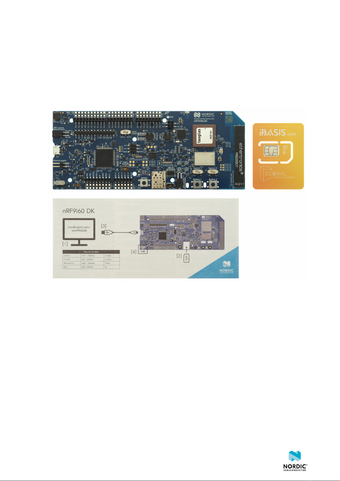
The nRF9160 DK (PCA10090) comes with a GPS antenna and a SIM card.
Figure 1: nRF9160 DK kit content
Hardware files
The hardware design files including schematics, Printed Circuit Board (PCB) layout files, bill of materials,
and Gerber files for the nRF9160 DK are available on the product page.
4418_1216 7

3Operating modes
The nRF9160 DK has various modes of operation.
3.1 Firmware development mode
The firmware development mode is the default with the IFMCU DISCONN switch (SW6) in the left position.
The primary interface for programming and debugging the nRF9160 DK is the USB port (J6). The USB port
is connected to an interface MCU which embeds a SEGGER J-Link-OB (On Board) debug probe.
Figure 2: nRF9160 DK firmware development mode
3.1.1 Device programming
The nRF9160 DK supports Serial Wire Debug (SWD) programming interfaces for both onboard and off-
board nRF targets.
The primary target for programming and debugging in the DK is the nRF9160 SiP. The interface MCU also
supports programming the onboard nRF52840 as well as external nRF devices fitted on a shield or through
a connector to external boards such as the user's own prototypes.
The interface MCU will automatically detect if external targets are plugged in. The PROG/DEBUG switch
(SW10) is used to select nRF9160 or nRF52840 for programming or debugging on board. Note that there
are significant limitations on using the nRF52840 on the nRF9160 DK. For more information, see nRF9160
DK board control on page 20.
3.1.2 Virtual COM port
The interface MCU also features three UART interfaces through three virtual COM ports.
The virtual COM ports are the following:
• VCOM0 – Connected to nRF9160 (default)
• VCOM1 – Connected to nRF52840 (nonconfigurable)
• VCOM2 – Connected to nRF9160 (default)
For details on routing VCOM0 and VCOM2, see nRF9160 DK board control on page 20.
The virtual COM ports have the following features:
• Flexible baud rate settings up to 1 Mbps
4418_1216 8

Operating modes
•Request to Send (RTS)/Clear to Send (CTS)-style Hardware Flow Control (HWFC) handling
The following table shows an overview of the General-Purpose Input/Output (GPIO)s used for the UART
connections on nRF9160 and nRF52840:
nRF91 APP1 nRF91 APP2 nRF52840
TXD P0.29 P0.01 P0.03
RXD P0.28 P0.00 P0.05
CTS P0.26 P0.15 P0.07
RTS P0.27 P0.14 P1.08
Table 1: GPIOs used for virtual COM ports on nRF9160 and nRF52840
Note:
• Baud rate 921 600 is not supported through the virtual COM port.
3.1.3 MSD
The interface MCU features a Mass Storage Device (MSD). This makes the DK appear as an external drive
on your computer.
This drive can be used for drag-and-drop programming. However, files cannot be stored on this drive. By
copying a HEX file to the drive, the interface MCU will program the file to the device. The J-Link OB will
program the target that is selected with the nRF52/nRF91 switch (SW10). For limitations on nRF52840 use,
see nRF9160 DK board control on page 20.
Note:
• Windows might try to defragment the MSD part of the interface MCU. If this happens, the
interface MCU will disconnect and become unresponsive. To return to normal operation, the DK
must be power cycled.
• Your antivirus software might try to scan the MSD part of the interface MCU. Some antivirus
programs trigger a false positive alert in one of the files and quarantine the unit. If this happens,
the interface MCU will become unresponsive.
• If your computer is set up to boot from USB, it can try to boot from the if the DK is connected
during boot. This can be avoided by unplugging the DK before a computer restart or changing
the boot sequence of the computer.
You can also disable the MSD of the kit by using the msddisable command in J-Link Commander. To
enable, use the msdenable command. These commands take effect after a power cycle of the DK and
stay this way until changed again.
3.1.4 Reset
The nRF9160 DK is equipped with a RESET button (SW5).
By default, the RESET button is connected to the interface MCU that will forward the reset signal to the
nRF9160 SiP or nRF52840 System on Chip (SoC), depending on the state of the nRF52/nRF91 switch. If IF
MCU DISCONNECT is activated, the RESET button will be connected to the nRF9160 SiP directly.
4418_1216 9

Operating modes
3.2 Performance measurement mode
The performance measurement mode can be selected by moving the IFMCU DISCONN switch (SW6) to the
right position, which disconnects the interface MCU from the nRF9160 SiP using analog switches.
This is done to isolate the nRF9160 SiP as much as possible and can be of use when measuring currents on
low-power applications.
Figure 3: nRF9160 DK performance measurement mode
The DK detects if there is a USBUSB cable plugged in (see USB detect on page 10) and will disconnect
and power down the interface MCU when another supply than the USB is used. If the USB connector is
used for power supply only (USB battery back) you can also disable the interface MCU using SW6.
USB detect and SW6 also control the routing of the RESET signal from the RESET button (SW5). Normally, it
is routed through the interface MCU, but if that is disabled, the reset button will be routed directly to the
nRF9160 SiP.
There are also a number of other reset routing options available through the use of solder bridges:
• When the interface MCU is disconnected, the RESET button is connected to pin 32 (nRESET) of the
nRF9160 SiP. The RESET button can be disconnected from the nRF9160 SiP by cutting SB15.
• When the interface MCU is disconnected, shorting SB18 will connect the RESET pin of the Arduino
interface to the reset pin of the nRF9160 SiP.
• When the interface MCU is connected, shorting SB19 will connect the RESET pin of the Arduino
interface to the BOOT input of the interface MCU.
• Shorting SB16 will connect the RESET pin of the Arduino interface to the RESET button.
• Shorting SB17 will connect the RESET pin of the Arduino interface to the nRESET pin of the nRF9160 SiP.
• When the interface MCU is disconnected, shorting SB21 will connect the RESET pin of the nRF52840 to
the RESET button.
• Shorting SB22 will connect the RESET pin of the nRF52840 to the RESET button.
3.2.1 USB detect
To detect when the USB for the interface MCU is connected, there is a circuit sensing the VBUS of USB
connector J6.
When the USB cable is connected, the VDD is propagated to the USB_DETECT signal.
4418_1216 10
Autres manuels pour nRF9160
3
Table des matières
Manuels Matériel réseau populaires d'autres marques

Matrix Switch Corporation
Matrix Switch Corporation MSC-HD161DEL Manuel utilisateur

B&B Electronics
B&B Electronics ZXT9-IO-222R2 Manuel utilisateur

Yudor
Yudor YDS-16 Manuel utilisateur

D-Link
D-Link ShareCenter DNS-320L Manuel utilisateur

Samsung
Samsung ES1642dc Instructions d'utilisation

Honeywell Home
Honeywell Home LTEM-PV Instructions de montage