.""
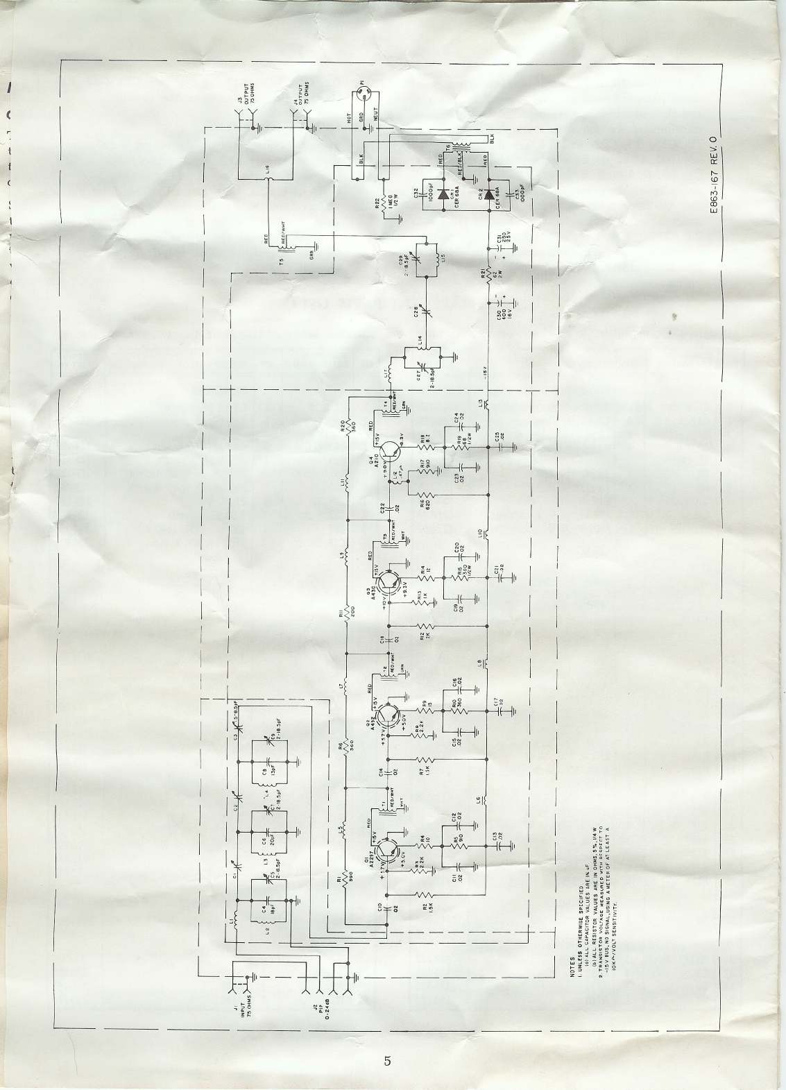
strips. Four NPN transistors are employed in a
cascaded common-emitter circuitry. All inter-stages
and the output stage have capacitors andJoroidal
transformers for impedance coupling: TI, .S;,JA;"""-
T2, CIS; T3, C22; and T4, are the components
involved. All stages have current feedback through
R4, R9, RI4, and RI8 respectively. Equally, all
stages have voltage feedba'Ck through RI, RB, Rll,
and R20 respectively. Base bias for each transistor
is developed across the relevant resistor pairs R2,
R3; R7, R8; RI2, RI3; and RIB, RI7. Again, tran-
sistor operating stability is achieved by RC net-
works: Cll, CI2, R5 tor QI; CI5, CI6, RIO for
Q2; CI9, C20, RI5 for Q3; and C23, C24, RI9
'IIfql£..Q4, in the respective emitter circuits.
4. OUTP.DT CIRCUITRY
From the collector of Q4 the output is inductively
coupled through LI7 to a 2"section bandpass Riter
consisting of series/parallel LC networks involving
C27, LI4, C28, C29, and LI5. This Riter too is
factory-tuned to the speciRed high-band channel.
From the RIter the signal is passed through T5 and
LIB which splits the signal energy. equally for
75-ohm impedance dual output presentation at
terminals J3 and J4.
J
.'iF"
ASSEMBLY,SMA-', HIGH-BAND REF. DWG. NO.: E863-167
REPLACEMENTPARTSLIST
REF. DWG. NO.: E863-166
~
ASSEMBLY: SMA-', LOW-BAND AND F.M.
..,--:::
"
..A\
"
4
SCHEMATIC JERROLO
ITEM liES/GNAT/ON QTY. DESCRIPTION PARTNO.
CAPACITORS
1C1,2,28 3prs. Variableplates, assembly 8215-289
2 C3 1 1.5-8.5pF,trimmer 128.572
3 C4 1 18pF,::!:5%,500V 124-079
4C5,7,9, 52-18.5pF,trimmer -128-570'
27,29
5 C6 120 pF,5%, 500V 124.119
6 C8 1 13 pF,5%, 600V 124-115
7 CI0thru25 16 0.02,uF,200V, disc 124.154
8 C30 1 400,uF,16 V, electrolytic 127-123
9C31 1 250,uF,25 V, electrolytic 127.062
CONNECTORS
10 11,3,4 3Chassisfitting Mod.F-61A
11 -3 Cableconnectors Mod.F-659
DIODES
12 CRl,2 2Rectifier,Silicon,CER68A S137.718
RESISTORS,
13 Rl 1 390O,5%, 1,4W 112.099
14 R2,7 21.5kO,5%, 1,4W 112-966
15 R3,8 22.2kO,5%,1,4W 112-932
16 R4 1 100, 5%, 1,4W 112.077
17 R5,17 29100, 5%,1,4W 112-920
18 R6,10,20 33600, 5%, 1,4W 112.098
19 R9 1150, 5%, 1,4W 112-973
20 Rll 1 2000, 5%, 1,4W 112-984
21 R12 1 2 kO,5%,1,4W 112-930
22 R13 11 kO,5%,1,4W 112.977
23 R14 1 12o, 5%, 1,4W 112-079
24 R15 1 300n, 5%, ¥2W 112-293
25 R16 1 6200, 5%,1,4W 112.998
26 R18 1 8.20, 5%,1,4W 112.075
27 R19 1 680, 5%,'12W112-212
28 R21 1620, 5%,2'Vl 112-211
29 R22 11MO,5%,1/2W 112-737
TRANSFORMER
30 T6 1 Linetransformer C141-264
TRANSISTORS
31 Ql 1 A2297 130-220
32 Q2 1 A492 130-185
33 Q3 1 A430 130-240
34 Q4 1 A210 130-200
SCHEMATIC JERROLD
ITEM DESIGNATION QTY. DESCRIPTION PARTNO.
CAPACITORS -
1Cl,2,18 31.5-8.5pF,trimmer 128.572
2C3,4, 5, 55-60 pF,trimmer 128.563
16,19
3C6thru C14 90.02 ,uF,200 V, disc 124-154
4C15 1 2-18.5pF,trimmer .. 128-570
5C17 1 400,uF,16V,electrolytic 127-123
6 C2o 1250JLF,25V,electrolytic 127-062
7C21,22 227pF,5% 124-120
8C23 15-60pF,trimmer 128-563
9 C24 1100pF,20%,1500V 124-101
10 C25,26 21000pF,200V,disc 124-020
CONNECTORS
11 JI,3,4 3Chassisfittings Mod.F-61A
12 -3Cable.fonnectors Mod.F.659
DIODES
13 CRl,2 2Rectifier,Silicon,CER68A S137.718
RESISTORS
14 Rl,6 21.5kO,5%,1,4W 112-966
15 R2 1 8200, 5%, 1,4W 112-976
16 R3,7 22.2kO,5%,1,4W 112-932
17 R4 120o, 5%,1,4W 112.083
18 R5 19100, 5%, 1,4W 1'12.920
19 R8 116o, 5%,1,4W 112.081
20 R9 13600, 5%, 1,4W 112-098
21 RIO 1 680n, 5%, 1,4W 112.105
22 R11 1 2 kn, 5%, 1,4W 112.930
23 R12 11kO,5%,1,4W 112-977
24 R13 1 300n, 5%, ¥2W 112.293
25 R14 1100n, 5%, lW 112-234
"'26 R15 ...!. 1 Mn, o, '12W112-743
TRANSFORMER
27 T4 1 Linetransformer 8141-251
TRANSISTORS
28 Q1 1A2297 130-220
29 Q2 1 A492 130-185
30 Q3 1 A43o 130.240