User guide 6 of 18 A
2022-04-26
RIC74424EVAL1 user guide
Open loop dual output gate driver with R9 FETs
Attention: Gate to source test points introduce small amounts of parasitic inductance, which increases
measured voltage overshoot and ringing. For critical measurements of amplitude and
settling time, it is recommended to place oscilloscope probes directly on gate and source pins
of the FET.
Table 5 Gate drive details
Channel FET Gate turn on resistor
(default populated)
Gate turn off resistor
(default not-populated)
Test point measurement
Positive (+) Negative (-)
A SMD-0.5/e (Q1) R4 R3 X7 pin 2 X7 pin 1
B SupIR-SMD (Q2) R10 R9 X21 pin 2 X21 pin 1
2.3.2 Power stage
RIC74424EVAL1 features two independent power stages, the first with a footprint supporting either SMD-0.5 or
SMD-0.5e package and the second with a footprint supporting SupIR-SMD package. These packages are
commonly used for a number of rad hard FET, such as rad hard R9 MOSFET and rad hard PowerMOS families.
The power stage is configured for a switching time test circuit, where a DC supply voltage is connected to the
drain of the FET through an external drain resistor. The intended operation is that a DC voltage is applied to the
power stage input connector, which is applied to the drain of the FET. The FET is then momentarily turned on,
which causes the drain voltage to decrease to about 0 V. The current through the channel of the FET is limited
by the drain resistor and FET drain to source on state resistance (RDS(on)). When the FET is turned off, the drain
voltage rises back to the DC supply voltage. This switching transition allows for rise and fall time
measurements. Capacitors are populated on both power stage inputs to help hold up the DC supply voltage
during this switching transition. If the FET or external resistance is changed, additional capacitance may be
needed.
The current through the channel of the FET is limited by the drain resistor. While this drain resistor are two
higher power rated devices in a 1210 package (500 mW each, for 1 W total), they are not intended to always be
on. If the FET is on too frequently these resistors can overheat and fail. As a result, it is recommended to limit
the frequency that the FET is on. This can be done by reducing the on-time pulse width and frequency when
on-time pulses occur. The exact limit depends on operating conditions, such as operating voltages and
ambient temperature, but general recommendation is to limit the on-time pulse width less than 10 µs and limit
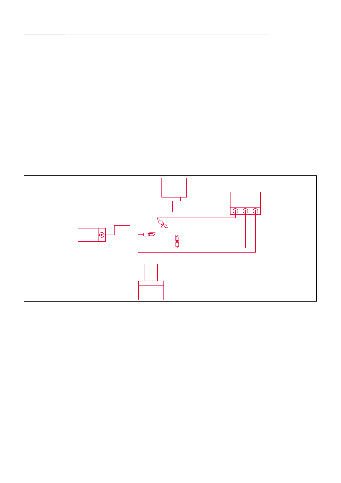
the frequency when the FET is on to greater than 10 ms. Details are shown in Figure 3. If the desired operating
times are close or exceed the recommended limits, it is recommended to slowly bring up the test while
measuring drain resistor temperature.
IN A
IN B
> 10 ms
< 10 µs
Figure 3 Timing diagram for recommended gate input signal