IEE 036X2-121-11120 Manuel utilisateur

APPLICATION REVISIONS
NEXT ASSY FINAL ASSY LTR DESCRIPTION DATE APPROVED
—Initial Release. E.O. 30328 94–07–26 B. Lo
ACorrect typos \ E.O. 30353 94–08–05 M. Englehart
BChange Cable Part No. \ E.O. 30367 94–08–15 B. Lo
CAdd –106 & –151 to Tables and Outlines, Revise
Section 4, Correct Typo Sht. 40 \ E.O. 31107 95–07–31 M. Englehart
DChange -105 Current Ratings on Sht. 16
\E.O. 31186
95–11–15 B. Lo
EAdd -120, -121, -130, -134 & -160 to Tables and
Outlines, Revise Section 4.4 Sht 29 \ E.O. 32196 96-11-7 B. Lo
FCorrect -105 Outline Dimensions \ E.O. 32330 96-12-4 B. Lo
GE.O. 32796 97-4-14 B. Lo
HE.O. 33653 98-4-3 B. Lo
JE.O. 34249 99-3-15 B. Lo
KE.O. 34831 99-11-23 B. Lo
LE.O. 34854 00-01-24 B. Lo
ME.O. 35324 00-05-30 B. Lo
NE.O. 35373 6-27-00 B. Lo
REV MG
SHEET 48 49 50 51 52 53 54 55 56 57 58 59 60 61 62 63 64 65 66 67 68 69 70 71
REV GGGGGGGGGGGLGGGGGGGGGNJG
SHEET 24 25 26 27 28 29 30 31 32 33 34 35 36 37 38 39 40 41 42 43 44 45 46 47
REV N N GGGGGGGGGGGGGGGGHHG G G G
SHEET CV
R1 2 3 4 5 6 7 8 9 10 11 12 13 14 15 16 17 18 19 20 21 22 23
REVISION STATUS
PROJ. NO. 346 CONTRACT INDUSTRIAL ELECTRONIC ENGINEERS, INC.
VAN NUYS, CALIFORNIA
NOTICEISHEREBYGIVENTHATTHISDRAWING
ISPARTOFAPROPRIETARYITEMOWNEDBY
INDUSTRIALELECTRONICENGINEERS,INC.AND
Specification, VFD, Century Series,
SHALLNOTBEREPRODUCED,ORCOPIEDORUSEDASTHE
BASISFORMANUFACTUREOR
SALEOFAPPARATUSWITHOUTWRITTEN DRAWN M. Englehart 07–26
Dot Matrix Modules
PERMISSIONOFIEE,INC. CHECK D. McCoy 07–26
APPROVED SIZE CODE IDENT NO.
B. Lo / 94–07–26 A05464 S036X2
APPROVED SCALE None SHEET 1OF 49

REV. N
PRODUCT SPECIFICATION
Century Series Flip
Dot Matrix ASCII VFD Modules

Industrial Electronic Engineers, Inc. SIZE
ACODE IDENT NO.
05464 S036X2–XXX–XXXXX
Van Nuys, California SCALE N/A REV NSHEET 2of 49
04/10/02
TABLE OF CONTENTS
LIST OF ILLUSTRATIONS ................................................................................................................................3
LIST OF TABLES............................................................................................................................................4
DEFINITIONS AND CONVENTIONS..................................................................................................................5
1.0 SCOPE.....................................................................................................................................................6
2.0 APPLICABLE DOCUMENTS.......................................................................................................................6
3.0 CHARACTERISTICS ..................................................................................................................................6
3.1 GENERAL....................................................................................................................................................6
3.1.1 Environment................................................................................................................................6
3.1.2 Useful Life ..................................................................................................................................6
3.1.3 Display Functions .......................................................................................................................6
3.1.4 Size and Weight .......................................................................................................................10
3.1.5 Character Cell Features .............................................................................................................10
3.1.6 Character Font Data..................................................................................................................11
3.2 INTERFACES ..............................................................................................................................................17
3.2.1 Power Interface.........................................................................................................................17
3.2.2 Data Interface...........................................................................................................................18
3.2.2.1 Serial ....................................................................................................................................18
3.2.2.2 Parallel..................................................................................................................................18
3.2.3 Personality Interface..................................................................................................................18
3.2.4 Power/Data Connector...............................................................................................................19
3.3 PERFORMANCE CHARACTERISTICS..................................................................................................................21
4.0 PROGRAMMING CODES.........................................................................................................................25
4.1 NUMERIC ORDER CONTROL CODES .................................................................................................................25
4.2 CURSOR CONTROL CODES ...........................................................................................................................27
4.3 DATA DISPLAY MODE CODES .......................................................................................................................28
4.4 PREPARE TO READ CODES ...........................................................................................................................30
4.5 SCREEN CONTROL CODES ............................................................................................................................31
4.6 MISCELLANEOUS CODES ..............................................................................................................................33
4.7 LCD MODE CONTROL CODES (WITHOUT INTERFACE CONVERTER).........................................................................35
4.8 UNSUPPORTED LCD CONTROL CODES (WITHOUT INTERFACE CONVERTER)..............................................................35
4.9 LCD MODE CONTROL CODES (WITH INTERFACE CONVERTER)..............................................................................36
4.10 UNSUPPORTED LCD CONTROL CODES (WITH INTERFACE CONVERTER).................................................................36
5.0 OPTIONS AND ACCESSORIES................................................................................................................37
5.1 PERFORMANCE OPTIONS ..............................................................................................................................37
5.2 ACCESSORIES............................................................................................................................................37
6.0 OUTLINE DRAWINGS..............................................................................................................................38

Industrial Electronic Engineers, Inc. SIZE
ACODE IDENT NO.
05464 S036X2–XXX–XXXXX
Van Nuys, California SCALE N/A REV NSHEET 3of 49
04/10/02
LIST OF ILLUSTRATIONS
Figure Description Page
3–1 Functional Block Diagram, Intel Mode ........................................................................... 7
3–2 Functional Block Diagram, Motorola Mode ............................................................... 8
3–3 Functional Block Diagram, LCD Mode ............................................................................ 9
3–4 ASCII Character Set ..................................................................................................... 12
3–5 Cyrillic Character Set ..................................................................................................... 13
3–6 European Character Set ......................................................................................... 14
3–7 Hebrew Character Set ..................................................................................................... 15
3–8 Katakana Character Set ..................................................................................................... 15
3–9 LCD (Hitachi) Character Set ......................................................................................... 16
3–10 Personality Jumper Positions ......................................................................................... 19
3–11 J1 Contact Arrangement ......................................................................................... 19
3–12 Timing Characteristics, Intel Mode ............................................................................. 22
3–13 Timing Characteristics, Motorola Mode ............................................................................. 23
3–14 Timing Characteristics, LCD Mode ............................................................................. 24
6–1 Outline Drawing, 036X2–100–05420 ............................................................................. 39
6–2 Outline Drawing, 036X2–105–05220 ............................................................................. 40
6–3 Outline Drawing, 036X2–106–04240 ............................................................................. 41
6–4 Outline Drawing, 036X2–120–09120 ............................................................................. 41
6–5 Outline Drawing, 036X2–121–11120 ............................................................................. 42
6–6 Outline Drawing, 036X2–122–09220 ............................................................................. 44
6–7 Outline Drawing, 036X2–124–09420 ............................................................................. 45
6–8 Outline Drawing, 036X2–130–11220 ............................................................................. 45
6–9 Outline Drawing, 036X2–134–11420 ............................................................................. 46
6–10 Outline Drawing, 036X2–151–05240 ............................................................................. 48
6–11 Outline Drawing, 036X2–160–05440 ............................................................................. 48

Industrial Electronic Engineers, Inc. SIZE
ACODE IDENT NO.
05464 S036X2–XXX–XXXXX
Van Nuys, California SCALE N/A REV NSHEET 4of 49
04/10/02
LIST OF TABLES
Table Description Page
3–1 Physical Dimensions ...................................................................................................... 10
3–2 Display Character Fonts ...................................................................................................... 11
3–3 Display Supply Current ...................................................................................................... 17
3–4 Connector Pin Assignments .......................................................................................... 20
3–5 Execution Times ....................................................................................................... 21
4–1 Dot Data for User Defined Characters ............................................................................... 29

Industrial Electronic Engineers, Inc. SIZE
ACODE IDENT NO.
05464 S036X2–XXX–XXXXX
Van Nuys, California SCALE N/A REV NSHEET 5of 49
04/10/02
DEFINITIONS AND CONVENTIONS
Conventions:
⇒First Line, Column, Bit or Position is 0 or 00h.
⇒Control Code names are italicized.
⇒Upper case A with subscript from 0 to 7 indicates an address bit from LSB to MSB.
⇒Upper case D with subscript from 0 to 7 indicates a data bit from LSB to MSB.
⇒Counting order is left–to–right, top–to–bottom.
⇒Hexadecimal notation is represented as XXh, where X is a numeric 0 – 9, or alpha A – F.
⇒X = “Don’t Care” or Variable Data
Definitions:
Attributes Blink or Brightness Level.
Field A display screen area consisting of one or more characters having attributes set.
Home First line, first column; display screen position 00h.
Reset Return display or function to its baseline (default condition).
Restore Return display or function to a previously established state.
Abbreviations:
AAmperes LSB Least Significant Bit
AnAddress ‘n’ mA Milliamperes
AC or ac Alternating Current max Maximum
ASCII American Standard Code for Information Interchange min Minimum
oCDegrees Centigrade (Celsius) mm Millimeters
CG Character Generator Mot Motorola
CG RAM Character Generator RAM MSB Most Significant Bit
CR Carriage Return msec Milliseconds
CS Chip Select nsec Nanoseconds
DnData Bit ‘n’ oz Ounces
DC or dc Direct Current RAM Random Access Memory
DD RAM Data Display RAM RD Read
EEnable RS Register Select
EIA Electronic Industries Association RST Reset
ft–L Foot–Lamberts µAMicroamps
gGravitational Units µFMicrofarads
Hz Hertz (Cycles per Second) µsec Microseconds
ID Identity or Identification UDC User Defined Character
I/O Input/Output VVolts
LCD Liquid Crystal Display VFD Vacuum Fluorescent Display
LF Line Feed WR Write

Industrial Electronic Engineers, Inc. SIZE
ACODE IDENT NO.
05464 S036X2–XXX–XXXXX
Van Nuys, California SCALE N/A REV NSHEET 6of 49
04/10/02
1.0 SCOPE
This document describes the complete performance and interface characteristics of the dot matrix family of
Century Series Vacuum Fluorescent Displays (VFD). For the remainder of this document, the Century
Series VFDs are referred to as the display.
2.0 APPLICABLE DOCUMENTS
The following documents form a part of this specification to the extent specified herein.
EIA–232 Interface Between Data Terminal Equipment and Data Communication Equipment
Employing Serial Binary Data Interchange
3.0 CHARACTERISTICS
3.1 General
The following sections describe the basic or “Standard” Century Series Dot Matrix VFD. For a complete list
of options and accessories, see Paragraph 5.0.
3.1.1 Environment
The display will operate properly following exposure to any combination of the listed environmental
conditions:
Storage Temperature –50oC to +85oC
Operating Temperature –20oC to +70oC (Normal) -40oC to +85oC (Wide)
Relative Humidity 0 to 90% (Non–condensing)
Vibration 10 to 500 Hz, 2 mm Peak–to–Peak (any axis)
Shock 20 g (any axis)
3.1.2 Useful Life
The useful life of the displays ranges from 40,000 to 100,000 hours.
NOTE
Useful life for a vacuum fluorescent tube is defined as the period over which
the light output decreases to half of its specified initial minimum
brightness. Maximum useful life is achieved by display of random text
messages. Users are encouraged to avoid fixed messages wherever
possible, and to clear or blank the display when not in use. A screen
saver mode is provided.
3.1.3 Display Functions
The dot matrix family of Century Series VFDs is able to simulate Intel 8041/42 series, Motorola 6821 and
Hitachi 44780 interface characteristics as specified herein.
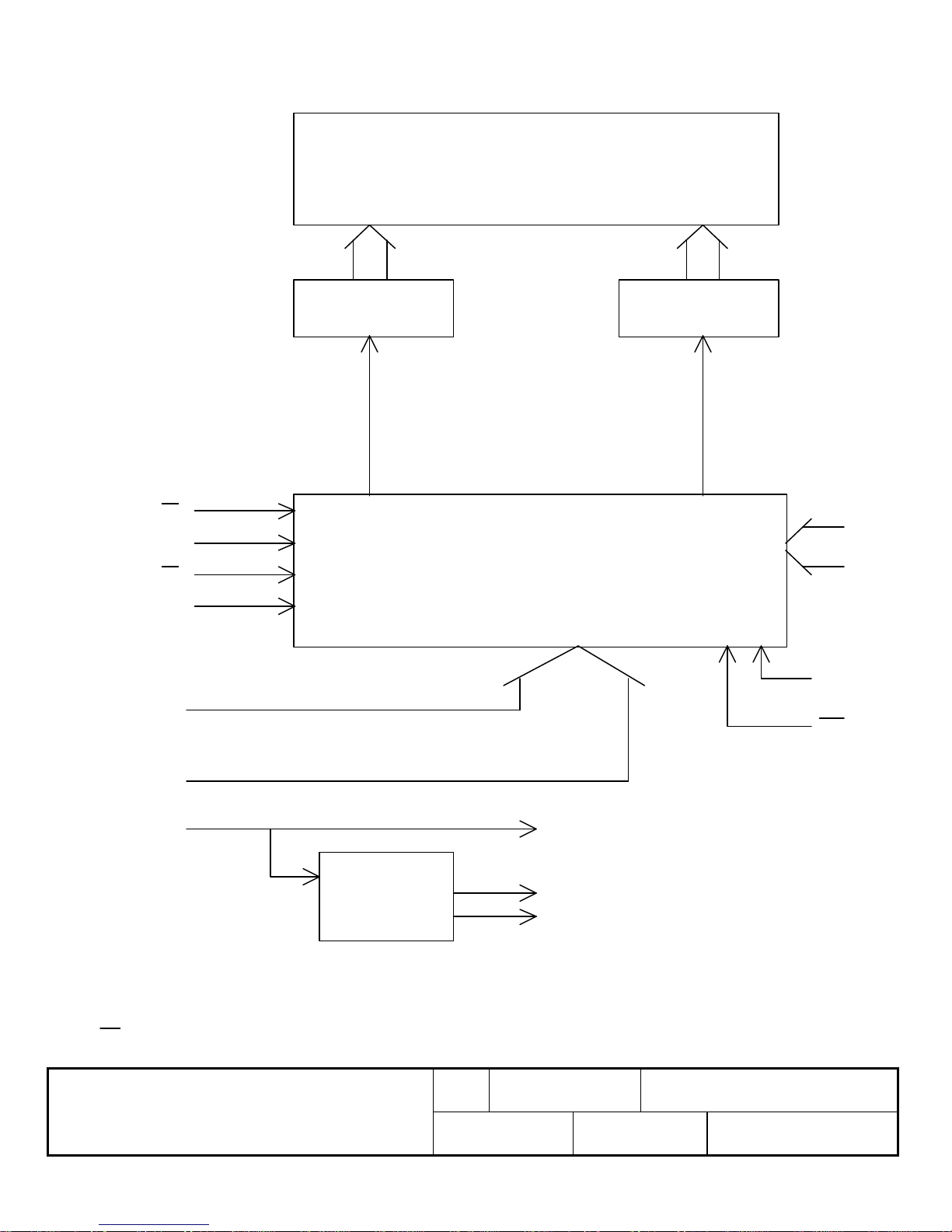
Critical interface lines are shown in the functional block diagrams, Figures 3–1, 3–2 and 3–3.

Industrial Electronic Engineers, Inc. SIZE
ACODE IDENT NO.
05464 S036X2–XXX–XXXXX
Van Nuys, California SCALE N/A REV NSHEET 7of 49
04/10/02
Display Tube
Anode
Drivers GridDrivers
Microcontroller
WR
RD
A0
CS
Control
Serial
Input
8-Bit
Bidirectional
Data Bus
DC to DC
&
DC to AC
Voltage
Converter
+5 Vdc
Jumpers
DIMMING
(Hardware)
RST
BUSY
(Not used in Serial Mode)
(Row) (Column)
Logic Supply
Filament Supply
Anode/Grid Supply
(Not used in Serial Mode)
BELL
Figure 3–1
Functional Block Diagram, Intel Mode

Industrial Electronic Engineers, Inc. SIZE
ACODE IDENT NO.
05464 S036X2–XXX–XXXXX
Van Nuys, California SCALE N/A REV NSHEET 8of 49
04/10/02
Display Tube
Anode
Drivers GridDrivers
Microcontroller
RD/WR
CS
Control
Serial
Input
8-Bit
Bidirectional
Data Bus
DC to DC
&
DC to AC
Voltage
Converter
+5 Vdc
Jumpers
DIMMING
(Hardware)
RST
BUSY
(Not used in Serial Mode)
(Row) (Column)
Logic Supply
Filament Supply
Anode/Grid Supply
E
RS
(Not used in Serial Mode)
BELL
Figure 3–2
Functional Block Diagram, Motorola Mode

Industrial Electronic Engineers, Inc. SIZE
ACODE IDENT NO.
05464 S036X2–XXX–XXXXX
Van Nuys, California SCALE N/A REV NSHEET 9of 49
04/10/02
Display Tube
Anode
Drivers GridDrivers
Microcontroller
RD/WR
CS
Control
8-Bit
Bidirectional
Data Bus
DC to DC
&
DC to AC
Voltage
Converter
+5 Vdc
Jumpers
DIMMING
(Hardware)
RST
(Row) (Column)
Logic Supply
Filament Supply
Anode/Grid Supply
RS
E
Figure 3–3
Functional Block Diagram, LCD Mode
Note:
CS
must be grounded when using LCD Mode.
Ce manuel convient aux modèles suivants
10
Table des matières
Autres manuels IEE Échelle