ROSE COMPARISON OF AUDIO POWER AMPLIFIERS
AES 112
TH
CONVENTION, MUNICH, GERMANY, 2002 MAY 10–13 4
6.3. Continuous output power
The input to the amplifier, a fixed frequency sinewave, was ramped
up slowly and the power output and THD+N were recorded in a
21kHz bandwidth set by an AES17 20kHz brickwall filter. At
58Hz, each amplifier was tested with 4Ωresistive, 8Ωresistive,
and loudspeaker loads. In the case of the loudspeaker load, the
measured power is based on the amplifier output voltage and the
real part of the loudspeaker impedance (5.06Ω) to measure the
power dissipated in the driver. Other test frequencies were chosen
to cover the rest of the audio band. 1kHz was chosen because it is a
standard frequency for testing, 7kHz was chosen as the highest
frequency that has the third harmonic in a 21kHz bandwidth. 14
kHz was chosen because it represents the high end of the audio
bandwidth and its third harmonic is within 42kHz, another standard
AES17 filter bandwidth. The assumption made here was that the
harmonics would decrease in amplitude as their order increases and
the THD+N level as measured from these is representative of the
true unlimited bandwidth values.
At 1kHz, 7kHz and 14kHz, the loads used were 4Ωresistive and
8Ωresistive. In the 14kHz case, the measurement system
bandwidth was increased to 42kHz by using an AES17 40kHz
brickwall filter
The output power for 0.1% and 1% THD+N was recorded to the
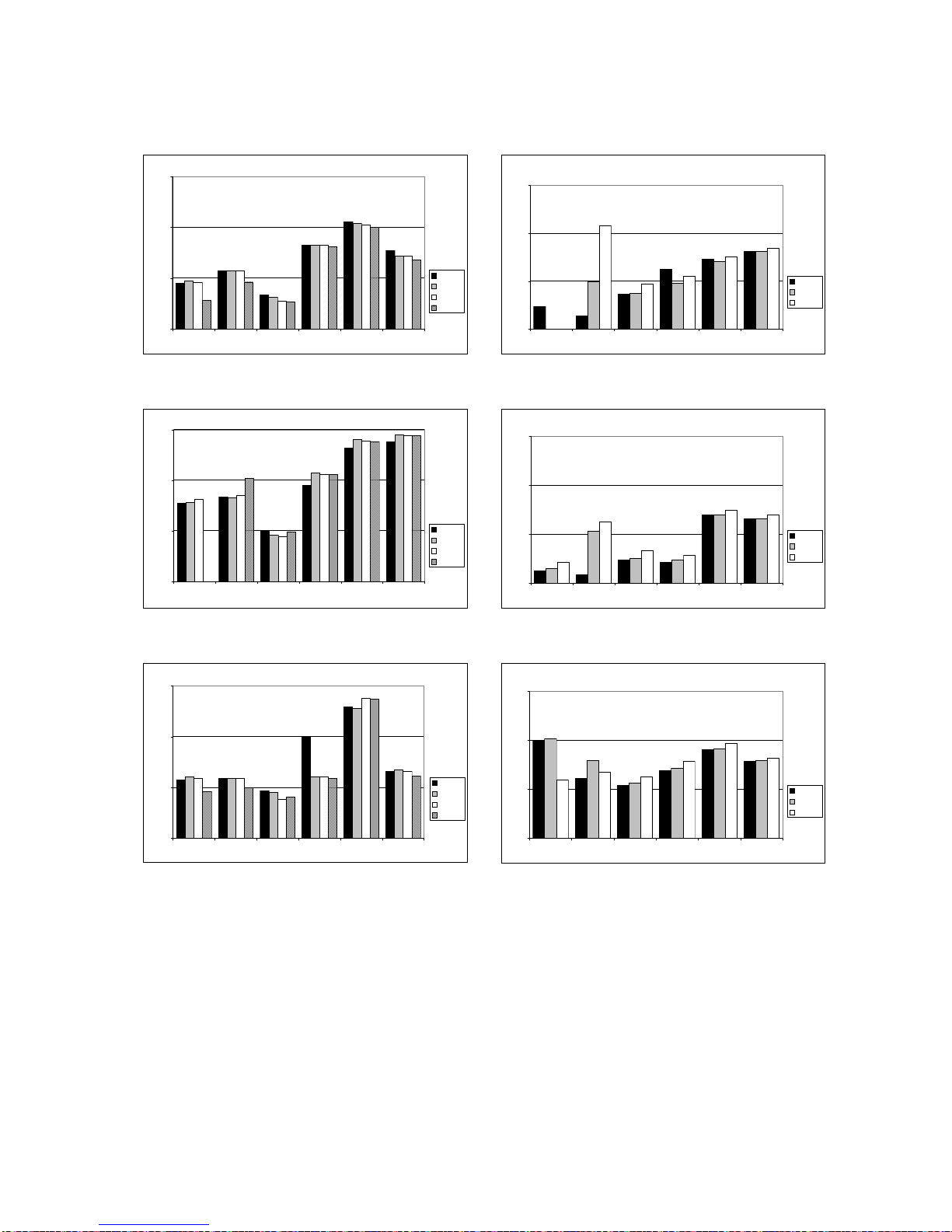
nearest 0.5W. The comparisons of results can be seen in appendix
A where Figs. 1-9 show continuous power outputs of the amplifiers
with different power supplies, at different frequencies and with
different loads.
Figs. 10-18 in appendix A show the value of the amplifier, heatsink
and power supply combination in terms of the output power. This
could be considered the measure of “bang for the buck”, or a
measure of value for money. They are shown as 10log(power/total
cost) for simple viewing. The total cost has been normalised to the
cost of amplifier 1 with a 60VA unregulated power supply.
6.4. Distortion at a known power
Using the data generated in section 6.3., it is possible to read the
THD+N at any output power. The power chosen was the power
when the output voltage swing is ±17.5V, half the theoretical
lossless maximum. This corresponds to 19W into an 8Ωresistive
load, 38W into a 4Ωresistive load, and 30W into the real part of
the loudspeaker load at 58Hz. The results are seen in the appendix
B, figs. 1-9.
To compare the value of the amplifiers in terms of their distortion,
the THD+N was multiplied by the total cost of the amplifier,
heatsink and power supply combination. The costs were
normalised to the cost of amplifier 1 with the 60VA unregulated
power supply. The results are shown in appendix B, figs. 10-18.
7. RESULTS AND DISCUSSION
7.1. Noise
This section discusses table 2. The lowest absolute output noise
voltage and EIN are shown by the TFHs (amplifiers 3 and 4). The
switch mode amplifiers (5 and 6) show the poorest noise
performance. Amplifier 2, an IC, comes close to the EIN
performance of the TFHs.
In most cases, higher output noise also means higher EIN, but in
the case of amplifier 1, with quite low output noise the EIN is quite
high because of its low gain. The noise performance of linear
amplifier modules, particularly TFHs is currently better than that of
switch mode amplifier modules.
7.2. Value In Terms Of Noise
This section discusses table 2. If EIN multiplied by normalised cost
is an inverse measure of value, then the TFH power amplifier
modules (3 and 4) have the highest value, followed by the ICs (1
and 2). The switch mode amplifiers (5 and 6) are considerably
lower in value. In terms of noise performance, linear amplifiers
currently offer higher value than switch mode amplifiers. Among
linear amplifiers, TFHs offer more value than ICs.
7.3. Continuous Output Power
This section discusses the main features of figs. 1-9 in appendix A.
The continuous power output performance of the IC amplifiers (1
and 2) is often degraded by their protection circuitry, particularly at
low frequencies with a 4Ωresistive load. Some data could not be
measured for amplifier 1 at high frequencies because it is unstable
and the measurement sweep could not be completed. Data are also
missing for amplifier 5 at high frequencies at 0.1% THD+N
because the output at all power levels had greater than 0.1%
THD+N. In terms of continuous power output, the amplifiers
perform similarly with the 8Ωresistive load at 1kHz and 7kHz.
These results are particularly interesting for two reasons. Firstly,
linear amplifiers perform similarly while switch mode amplifiers
show clearly different output power to each other. This suggests
that switch mode technology is not as mature as linear technology
because the optimum performance has not been found by all
manufacturers. Secondly, the most common use of switch mode
amplifiers is as bass amplifiers, but these results suggest that their
efficiency advantage over linear amplifiers is greater at high
frequencies.
With the loudspeaker load at low frequencies, the performance
comparison resembles the performance comparison with the 8Ω
resistive load. When the supply voltage is kept constant, the
maximum output power from any non-protecting amplifier
increases with the VA rating of the transformer. The output of the
TFH amplifiers appears to almost double from the 60VA
unregulated power supply to the regulated supply. In many cases,
the switch mode amplifiers show a higher output than the linear
amplifiers when using the lower rated supplies. This is particularly
the case at higher frequencies, with the 4Ωresistive load, and at the
1% THD+N level. It is caused by the greater efficiency of the
amplifier topology.
The IC amplifiers (1 and 2) do not always show a higher
continuous power output when used with a larger power supply,
and they do not perform as well as TFHs with low impedance
loads. The TFH amplifiers (3 and 4) show the most consistent
output capacity at different frequencies. One of the switch mode
amplifiers has higher output at low frequencies, while the other has
higher output at higher frequencies.
7.4. Value In Terms Of Continuous Output Power
This section discusses figs. 10-18 in appendix A. In this section,
high value means high continuous output power to cost ratio.
With all loads, and at all frequencies, it can be seen that the linear
amplifier solutions (1-4) offer the highest value, and show similar
performance. Switch mode amplifier 5 offers less value, and
amplifier 6 offers considerably less.
At low frequencies with the 4Ωresistive load, amplifier 1 offers
lower value for higher VA rated power supplies. This is because its
internal protection circuitry reduces the available output power.
At low frequencies, the amplifiers offer similar value for both 0.1%
and 1% THD+N levels. At higher frequencies, the value at the
0.1% THD+N level is very much lower for some amplifiers
because of increased distortion levels. Switch mode amplifier 5 is
the most affected by this phenomenon.
In the case of an amplifier functioning normally with no adverse
protection circuitry effects, value with different transformers is
similar. This suggests that a larger transformer is money well spent.
When looking for the optimum transformer rating, in most cases,
the 120VA transformer offers the highest value. This is a
combination of the higher performance and low cost increase
compared to the 60VA power supply. This suggests that for any
given power supply voltage and load, there is an ideal transformer
rating to give optimum value.