Becker europa TR Manuel utilisateur

Service Manual
A-1 valid BEZW (24 volt type)
devices Technology C / 08 from
device 700. 000th A 50001


Table of Contents
page 3 Operating Features and Specifications
page 4 Image for Operating Features
page 5 Electrical function description AM bands
page 6 Electrical Function Description FM areas
page 7 Electrical function description LF section
page 7 Voltage switching polarity switching
page 8 Mechanical design and function
Page 9, 10th , , , ldungen Device Abbi
page 11 Notes for mechanical adjustment and repair work
page 13 Conversion process for connecting a record player or tape recorder
page 14 Technical data of the Mikrofonvorsetzers
page 14 Note on the minibus system with microphone connection Printed circuit
boards
page 15 UK-plate
page 19 RF to IF plate
page 23 NF-plate
page 26 level diagram
page 27 General calibration instructions
page 28 LF part Europe TR 24 Volt
page 29 Clean Tools
page 30 Adjustment positions
page 31 balance manual
page 32 Diagram Europe TR LMKU
page 33 Diagram Europe TR LMKU 24 Volt
page 34 Parts List (electrical parts) HF-IF section
page 36 Parts List (electrical parts) NF-Tei l
page 38 Parts List (mechanical parts)

Operating Features and Specifications
Tuning: range setting:
Fade:
Connection options:
Operating voltage:
means variometer vote on pushbuttons.
Possibility to lock stations (1 x LW, MW 1 x, 1 x KW, 2 x FM)
2-stage
1 or 2 speakers shortwave adapter "Reims
8" automatic antenna
switchable to request connection for car turntable or tape recorder (for recording and
playback) to 6 V or 12 V plus or minus to ground
Technical specifications
wavebands
LMK FM
Frequencies
145-400 kHz
510-1630 kHz
5.9 to 6.25 MHz
87-108 MHz
variable circles
3
3
1
2
solid circles
5
5 7
11
Intermediate Frequency:
Shrinkage control:
Scales lamp: Assembly:
AM 460 kHz FM 10.7 MHz
effective over 2 steps 7 V / 0.1 A
transistors
diodes
Receiver 2 x
106 4 x AF AF
138
4 x 3 x AA112
AA119
NF-part 1 x 125
1 x AC AC AC
126 1 x 128 2 x
148 1 x AD St 1
to stabilize internal voltages diodes:
1 x 2.1 10 St 1 x
100 BZ
Quiescent current:
Talk performance:
Dimensions:
Weight:
0.3 A for 6 volts - Operating
0.29 A for 12 volt operation
>= 5 W at k total =
10%
Width
Height
Depth
2.7 kg
receiver part
180 mm 52
mm 150
mm
NF-part 180
mm 52
mm 83
mm
- 3 -

Fig. 1
1 connection cable between the device and LF section
2. LF part with end stage
3. receiver part
4. Manual tuning
5th hole for the adjustment of the antenna trimmer (below 750 mm seen against
device-back)
6. volume control, on-off (by rotation), tone control (in two stages, by -Zug to use)
Fig. 2
1. Antenna socket
2. plug (for connection Installation of turntable or tape recorders)
3. Ratio adjustment socket
4. Nameplate
5. connecting cable between the device and LF section
6. Power Cable
7. speaker connection plate (with two sockets for connecting any of a KW-adapter
"Reims 8" or an automatic Antenna e, f)
Explanatory note: A loudspeaker (5 Ω) between a-b connect. Two speakers (each 5 Ω) Explanatory note: A loudspeaker (5 Ω) between a-b connect. Two speakers (each 5 Ω) Explanatory note: A loudspeaker (5 Ω) between a-b connect. Two speakers (each 5 Ω) Explanatory note: A loudspeaker (5 Ω) between a-b connect. Two speakers (each 5 Ω)
between a-c and b-d
connect.
Before connecting a load to the socket e or f of the plastic plug must be removed
(by releasing the respective stud). The stud bolts are perpendicular to reach under
the sleeves e or f by the openings provided in the lid.
8. output transistors under the protection angle plate.
- 4 -

Electrical function description
1. AM bands KML
a) precursor
The antenna voltage is fed from the Trennkonden- sator C 1 (10 nF) to the input
circuit, which as for MW πKreis is designed. It is formed from the elements C 2 (An circuit, which as for MW πKreis is designed. It is formed from the elements C 2 (An
antenna trimmer with 10/60 pF) L 201 (input circuit variometer) and the series
connection of 203 C (170 pF) and 204 C (3 nF). Through the resistor R201 (180
ohms) can be the impedance curve ohms) can be the impedance curve
linearize. It also serves
the derivation of static charges. Possible low- frequency interference will be the
combination of R 202 (8,2 ohms), 204 C (3 nF) effective attenuated (see combination of R 202 (8,2 ohms), 204 C (3 nF) effective attenuated (see combination of R 202 (8,2 ohms), 204 C (3 nF) effective attenuated (see
KW of input circuit is fixed tuned. It is formed by the coil L and the antenna 204
Trimmer C 2 (10/60 pF) including the antenna intrinsic capacitance. The base of
the transistor precursors
inductively to this
Circuit coupled (see Fig. 5).
constricting resistance R 205 (2.2 ohms), by the C 207 (47 nF) constricting resistance R 205 (2.2 ohms), by the C 207 (47 nF)
is bridged for the HF.
Different mass points at the input circuit with C 2 (10 / 60pF) on the housing, R
201 (180 ohms), R202 (8.2 ohms), C 201 (20/100 pF), C 204 (3 nF), etc. are on the 201 (180 ohms), R202 (8.2 ohms), C 201 (20/100 pF), C 204 (3 nF), etc. are on the
inner negative pole by the
polarity switch due to battery voltage. The
collector side at the preliminary stage transistor lying off
agreed intermediate circuit is in turn adapted to the wave ranges as ML n-circle. In
conjunction with fol - constricting elements:
MW: C 210 (500 pF)
L 207 (variometer coil) 221 C (10/40
pF) C 220 (68 pF) in series with C 222
(1 nF) LW: C 210 (500 pF)
C 213 (5 nF) L 206 in series with L
207 C 220 (68 pF) C 222 (1 nF) C
219 (1.2 nF) C 223 (5 nF)
The collector current is supplied through R 209 (4.7 ohms) in parallel feed. The collector current is supplied through R 209 (4.7 ohms) in parallel feed.
KW for the intermediate circuit is provided as a fixed-tuned Vol circular l-
connected with L 205, C 211 (1.2 nF) in series with C 212 (200 pF). The basis of
the subsequent mixing stage is due to a partial capacity of this circle.
b) self-oscillating mixer
The oscillator and mixer function are met by the transit sistor T 202nd The
selectively comparable strengthened via the preamplifier input signal is conces-
via the respective divisional dependent capacitive divider based on T 202nd
Thus, the mixing transistor for the recom- works start signal
in the emitter circuit. For the oscillator chip
voltage is set by the base, the capacity of the divider condensers sufficiently low
impedance to the inner device masse, so that works in this case T 202 in the base
of circuitry, via the resistors R 214 (6.8 ohms) and R 226 (2.7 ohms) is biased, the of circuitry, via the resistors R 214 (6.8 ohms) and R 226 (2.7 ohms) is biased, the
base of the mixing transistor having a stabilized voltage part. the A
flow by temperature fluctuations and Exemplarstreu- Ungen wi rd through the
emitter resistor R 216 (2.7 ohms) reduced. emitter resistor R 216 (2.7 ohms) reduced.
be due to the collector of the transistor of the mixed The primary circuit of the first be due to the collector of the transistor of the mixed The primary circuit of the first
IF filter and the oscillator circuit. The IF circuit is tapped as the
Internal resistance of a
Mix stage in relation to the having a smaller value of an IF stage.
The oscillator circuit on MW Fig. 6 shows.
The RF precursor with T 201 operates in the usual emitter
circuit. To compensate for copy-scattering and temperature stabilization is Lie of
the emitter path
- 5 -
Fig. 3)
From the voltage divider C 203, C 204, the RF signal is applied to the base of the transistor T
two hundred and first
LW for the input circuit 202 as a full circle (LW-input circuit -Serienspule) works,
consisting of the series connection of L 201 (input circuit variometer) and L to the
C 2 (10/60 trimmer pF), C 201 (line trimmer 20/100 pF ) and the series connection
of 202 C (900 pF) and 204 C (3 nF) parallel to C 203 (170 pF), the circuit
capacitance form (see Fig. 4).
Fig. 4
Fig. 6
Fig. 5

iff a capacitive precipices the collector is of
T 202 at the oscillator circuit. The collector supply voltage wi rd through R 217 (47 ohms)T 202 at the oscillator circuit. The collector supply voltage wi rd through R 217 (47 ohms)
fed. The oscillator vibrates in three-point circuit. The series inductor L 215 is used
for narrowing the variation range, R 218 (33 ohms) to the oscillator variometer L for narrowing the variation range, R 218 (33 ohms) to the oscillator variometer L
216 linearizes the parallel resonant voltage over the areas. LW to the MW-OS 216 linearizes the parallel resonant voltage over the areas. LW to the MW-OS
zillator inductors (L 215, L 216) is connected the series coil L 218th The parallel
inductor L 217 is required to obtain a smooth running in LW. The oscillator
capacity wi rd in the LW range around 239 C (10/60 pF) + C 240 (440 pF)
increases. In KW-operation wi rd the inductances L 215, L 216, L 214 additionally
switched on as a parallel coil circuit capacitance as the capacitors of the divider
233 C (350 pF), C 234 (600 pF) are Merely effective.
c) IF gain c) IF gain
The following IF amplifier is 2-stage constructed
(T 203 and T 204). It contains the band filters F 202, F 204 and the individual
circuit L 225. The coupling of the low-basis via a respective capacitive divider ven.
The transistor T 203 is regulated. T 204 wi rd not regulated, so that it distort large
signal amplitudes can handle rungsarm.
d) Demodulation and control d) Demodulation and control
Signal and control means are concerned by the diode Di 206, which is inductively
coupled to the arrival last IF circuit. The resistors R 236 (3.3 ohms) + R 235 (6.8 coupled to the arrival last IF circuit. The resistors R 236 (3.3 ohms) + R 235 (6.8
ohms) form the load resistor. The NF is taken at R 235 (6.8 ohms) and supplied to ohms) form the load resistor. The NF is taken at R 235 (6.8 ohms) and supplied to
the volume control over C3 (0.1 microfarads). Through the resistors R 235 (6.8 ohms), the volume control over C3 (0.1 microfarads). Through the resistors R 235 (6.8 ohms),
R 236 (3.3 ohms) and R 230 (18 ohms) receives the base of the first transistor T R 236 (3.3 ohms) and R 230 (18 ohms) receives the base of the first transistor T
203 IF part of the stabilized through the diode Di 207 voltage as voltage
Grundvorspan-. The voltage drop across R 234 (390 Ω) biases diode Di 206 in Flow Grundvorspan-. The voltage drop across R 234 (390 Ω) biases diode Di 206 in Flow Grundvorspan-. The voltage drop across R 234 (390 Ω) biases diode Di 206 in Flow
direction before, thereby improving demodulators lation and
Demodulationsverzerrungen be Ringert comparable.
The in demodulation on the load resistor R 236 (3.3 ohms), R 235 (6.8 ohms) The in demodulation on the load resistor R 236 (3.3 ohms), R 235 (6.8 ohms)
resulting DC voltage is used for automatic uses gain control and R 230 (18 ohms), resulting DC voltage is used for automatic uses gain control and R 230 (18 ohms), resulting DC voltage is used for automatic uses gain control and R 230 (18 ohms),
R 225 (2.7 ohms) and R 219 (1 ohms) placed on the base of T 203rd The resulting
voltage diode clamping the basic prestress is opposed coupled ver thus a signal at
the incident Ringert the effective base bias of T 203. By thus verbun dene
lowering of the collector or emitter current will consequently the slope and thus the Gain lowering of the collector or emitter current will consequently the slope and thus the Gain
reduced. The emitter resistor R 222 (2.2 ohms) ent stationary voltage drop is used reduced. The emitter resistor R 222 (2.2 ohms) ent stationary voltage drop is used
for regulation of the pre-stage transistor T two hundred and first fal Since
transmission means l, the emitter current of T drops 203, the base bias of T 201
low, which also corresponds to a slope control of this transistor. the out Stabilization low, which also corresponds to a slope control of this transistor. the out Stabilization
reasons absolutely necessary emitter resistor R 205 (2.2 ohms) now exerts a reasons absolutely necessary emitter resistor R 205 (2.2 ohms) now exerts a reasons absolutely necessary emitter resistor R 205 (2.2 ohms) now exerts a
disadvantageous gen impact on the regulation since it any type of emitter current
change, so therefore also compensated by the control desired stabilizing effect.
This effect is the diode Di 201 in conjunction with the divider R 206 (680 Ω), R 207 This effect is the diode Di 201 in conjunction with the divider R 206 (680 Ω), R 207
(5.6 opposed ohms). In unge regulated state of the input transistor, the diode is
blocked, ie the measured against "inner Plus" clamping voltage drop at the emitter
branch R 205 (2.2 ohms) is greater than that from the divider 206 R (680 Ω), R 207 branch R 205 (2.2 ohms) is greater than that from the divider 206 R (680 Ω), R 207 branch R 205 (2.2 ohms) is greater than that from the divider 206 R (680 Ω), R 207
(5.6 ohms) Festge withstand voltage. In this operating case undergoes the (5.6 ohms) Festge withstand voltage. In this operating case undergoes the
transistor T 201 not influenced in its temperature stability through the diode
branch. however, Wi rd T 201 turned down, the emitter potential falls below
soon a value at which the diode Di opens wi 201 rd. This means for further down
rules that the precursor transistor wi tung kept almost constant Emitterschal- rd,
on which it has been switched on by diode Di 201 overall. So that the unwanted
DC negative feedback is canceled. Each additional increase of the RF input
voltage controls the level down further effective because changes in the control
voltage now vol l become effective on the base-emitter junction. In extreme cases,
the base potential of the emitter may up to even slightly positive, because the
emitter voltage of the controlled IF stage 203 to zero T
running. this chip
voltage also represents the control voltage for the transit sistor T two hundred and
first exceeded the down-regulated state
the control voltage, the temperature stabilization.
2. FM area
The FM input signal travels from the antenna via the AM-FM switch to the input of the
transformer Tr. 101. The input circuit formed with the secondary side of this
transformer is strongly attenuated and by the low input impedance of the pre-stage
transistor T 101 tuned to mid-band. In the collector branch of the transistor Lie
precursor gene by variometer (L 101) and a tunable intermediate circuit with the
voltage drop across R 102 (150 Ω) preloaded Damping diode Di 101, which prevents an voltage drop across R 102 (150 Ω) preloaded Damping diode Di 101, which prevents an voltage drop across R 102 (150 Ω) preloaded Damping diode Di 101, which prevents an
overdriving the mixing stage for large input signals comparable.
via the capacitor C 109 (4 pF), the amplified input signal reaches the emitter of the
self-oscillating mixer stage 102. The T
inductively tunable oscillator circuit loading
protrudes from the variometer L 102 and the circuit capacitance, Ge forms the trimmer
C 114 (3/10 pF) and the series connection of C 115 (18 pF) and C 116 (39 pF). The
feed- back a part of the oscillating voltage is done via C 113 (4 pF) to the emitter.
While the oscillator circuit to a capacitive Abgri the collector of the mixing stage ff is
the first 10.7 MHz IF circuit is performed fully on this transistor. That means:
for the oscillator frequency affects the IF
Coil as a high impedance choke through which the collector receives the operating
voltage. For the IF frequency, however, the relatively low-variometer coil L 102 is
parallel to the capacitors C 115 (18 pF) and C 116 (39 pF) to ground. The input and
output capacities,
in particular the
Oscillator and mixer transistor, are very dependent on the collector emitter voltage tor.
Therefore, the operating voltage by means of zener diode Di 208 was stabilized, the Di
to 208 connected in parallel electrolytic capacitor C 264 (50 uF) may seventh possible
low-frequency disturbances from the UK operating voltage. The IF voltage of the coil L
wi rd taken inductively 103 and the first filter F 101 supplied to the IF amplifier through
a coupling line (link line).
The subsequent amplification of the 10.7 MHz IF via four stages. The stages are
coupled via the bandpass filter F 202, F 203 and F 204 together. Al l IF stages are
neutralized, for reasons of stability. On the primary side of the filter 203 F wi rd
removed via C 225 (10 pF), a part of the ZF-voltage and in a chip
nungsverdopplerschaltung means of the diodes Di 202 and Di 203 used for generating
a control voltage. Via the resistor R 106 (2.2 ohms) reaches the control voltage a control voltage. Via the resistor R 106 (2.2 ohms) reaches the control voltage
clamping the base of the input transistor. If the demodulation of the IF signal
sym in the
trically constructed Ratio Filter F 205. Mi t means of the regulator R 241
(potentiometer. lin 3 kOhm.) can be possible tolerances in the ratio load resistors and (potentiometer. lin 3 kOhm.) can be possible tolerances in the ratio load resistors and
diodes compensate. The NF-signal passes through the deemphasis member R 240
(8.2 ohms), C 265 (68 nF), and is then about 3 C (0.1 uF) on Lautstärkereg- ler P. 1 (8.2 ohms), C 265 (68 nF), and is then about 3 C (0.1 uF) on Lautstärkereg- ler P. 1 (8.2 ohms), C 265 (68 nF), and is then about 3 C (0.1 uF) on Lautstärkereg- ler P. 1
- 6 -

3. NF gain
From the volume control the NF-voltage across C 301 (0.1 uF) reaches the input of the
transistor T 301. The high input resistance itself of this stage will now be greatly
reduced by the necessary basic divider. For this reason, it must How-through feedback
capacitor C 302 (2 microfarads) of the be lifted. Thus, the additional burden of the
demodulation stages is very low. In addition, the high input resistance for the
connectivity of a plate-tenspielers or tape recorder is desired.
The emitter resistor R 304 serving as an external resistance of the precursor and acts
at the same temperature-stabilizing effect. The second NF-T transistor 302 amplifies
the low-frequency signal in the emitter circuit. In this stage, the resistance R 309
unbridged linearized in frequency-dependent lung Stromgegenkopp- the course of the
amplification. The following driver stage T 303 must bring the control line up for the
push-pull output stage. At this stage the collector Treibertrans- is formator. Its
secondary winding drives the bases of the output transistors. To keep the distortion
low, wi the driver stage rd fed back into itself.
The NF-power output stage (T 304, T 305) working in push-pull B circuit with emitter
degeneration. The Kollektorruhe- current of 60 mA by means of wi rd R 318 is set. To
com- pensation one in the base chip temperature influences is voltage divider
lying NTC resistor. The influence possible
Licher voltage operating voltage variations on the basic advantages and
indirectly to the collector quiescent currents
is almost eliminated by acting as a stabilizer silicon diode Di three hundred and first
4. filtering, voltage switching polarity voters
The most important elements for the Liberation of interference from the electrical
system, the throttle D 1 and the Elektrolytkonden- sator C 5. The operating voltages of
the low signal levels suppressed by further filtering means and decoupled. Switching to
6 or 12 Volt operation takes place in the LF section. In this case corresponding contact
pins are bridged in the socket connector with a small repluggable contact plate. are
switched:
a) At the output transformer T 302, the collectors of the output transistors,
b) dividing the basis of the output stage R 319,
c) resistor for scale illumination R 320,
d) a series resistor for the operating voltage of all the small-signal stages R 316th
The device can be adapted to the vehicle battery larity means of a plug of the desired
Po. This requires additional change-over the housing-free guidance of the "inner
minus" or the "internal ground".
- 7 -

Mechanical design and function
The device EUROPA TR is 2-part, it consists of a receiver section (RF-IF part) and the
NF-part. The latter is screwed on in the normal fal l pivotally mounted on the receiver
part (fi gure 1 + 2). The LF section to be disposed of by the receiver part.
The tuning is done via the function keys of the printing unit and is possible in two
ways:
1. manual tuning,
2. The push-button voting.
Operation of the hand vote:
(For this purpose, see FIG. 7, 8 a, 8 b, 9, 10)
The hand drive shaft is provided with a screw WEL surface engages the hub located
on the drive wheel. A leaf spring presses the hand drive shaft against the thrust
bearing and in the drive gear, thus causing a play-free engagement of the tooth flanks.
The hub is ferrous ben the already mentioned driving wheel also riveted a frustoconical
clutch housing. The counterpart of the coupling is a triangular shaped clutch plate
screwed on the drive stud of the rocker
is.
The compound of the clutch is accomplished by a spring pressure. Upon rotation of the
hand drive shaft, the drive wheel wi rd moved, which pivots the rocker about its axis.
The rocker actuated thereby two voltage applied to its legs tongues which are
connected to the sled variometer and free of play comparable stressed by tension
springs 2. The vertical speed slide wi thus forced rd
Fastening screw of the abutment (AM 3 x 4
DIN 84)
thrust bearing
drive wheel
as moved. Wi around the drive turned to the left, the vertical speed cores dive into the
variometer coils with clockwise rotation they move in the opposite direction. In this
way, wi variable adjustment to the individual transmitters around causes.
Operation of the pushbuttons vote:
(For this, see Figures 7, 8 a, 8 b, 9, 10). The push buttons
have two functions:
1. Switching to different wavelength ranges (LW, MW, SW, FM) and
2. Determination of preferred stations for any repetition.
The station selection using the pushbutton following happens so:
First, wi the desired band around by actuating the corresponding push-button set. To
Kennt- lichmachung of the switched wave range remains the key pressed 2.5 mm back
are in the printing direction. The desired channel is now einge- by manual tuning sets,
the previously pressed pushbutton then until the stop is pulled out, therefore, the
previously set transmitter is fixed. Because now includes a well-defined position of the
vertical speed cores at any position of the rocker can once
fixed transmitter repeatedly by operating
the button can be set. This option is available once each in the LW, MW and SW area,
and twice in the VHF range. Fig. 8 a
Kupplungsglocke
Hand drive shaft
lifting flank
Fig. 8b
- 8th -
compression spring
release lever
Role in the release lever
Hexagonal nut (M 4
DIN 439 adjustment)
clutch disc
locking screw
"X"
"X"
Fig. 7
leaf spring
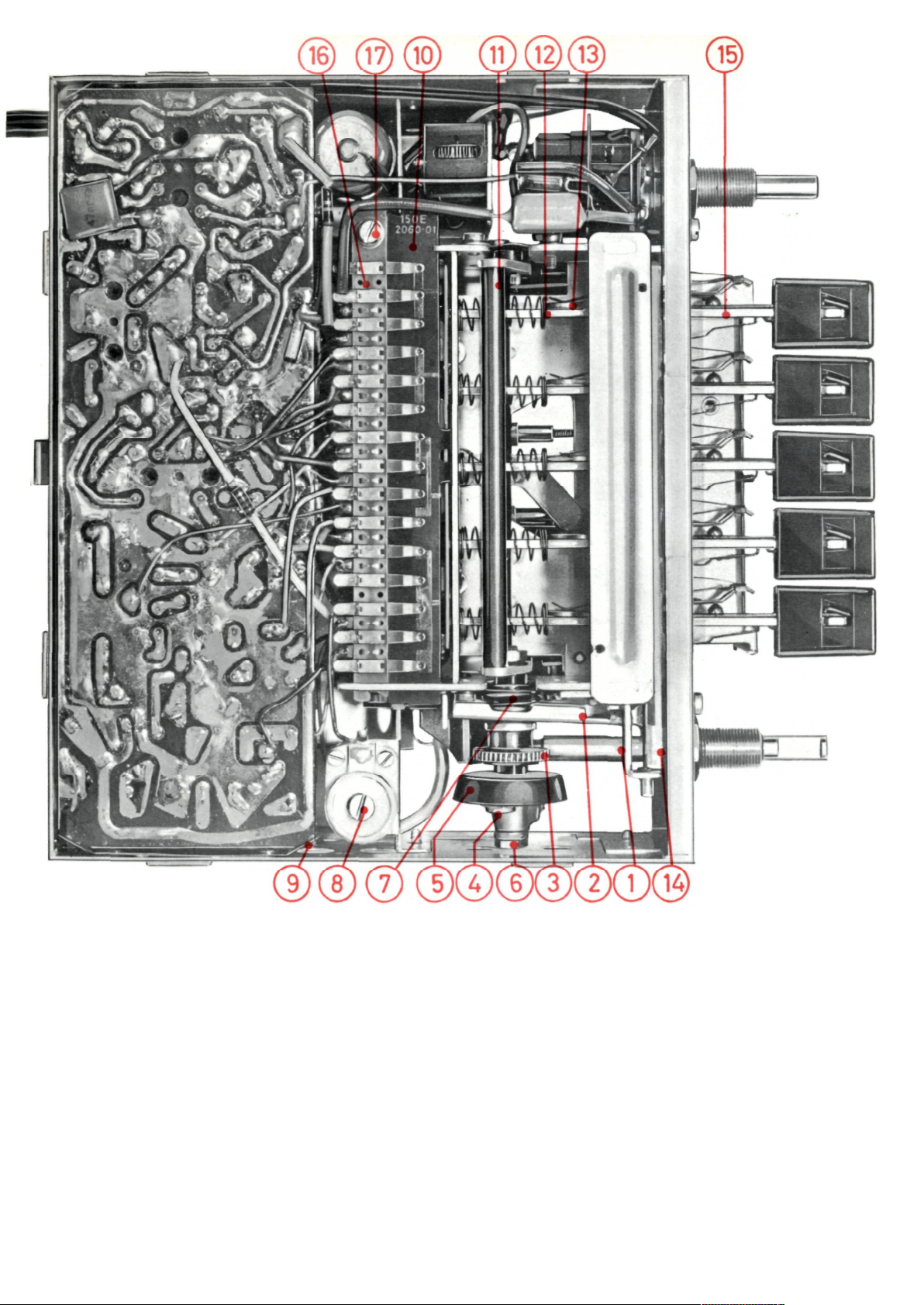
1. Hand drive shaft (see also Fig. 7 u. 8 a)
2. release lever
3. drive
4. clutch disc
5. Kupplungsglocke
6. adjusting nut M DIN 4 439 (see also Fig. 8a)
7. spring
8. Antenna Trimmer
9. retaining spring
10. Oil switch plate
11 rocker
12, return spring (to the shifting rod)
13. Segment (see also Fig. 11 b)
14 clutch comb
15 shift rod
16 wave switch I cpl.
17 cylinder head screw (at the shaft switch)
- 9 -
Fig. 9
Table des matières
Autres manuels Becker Radio

Becker
Becker BLU-BKR2 Manuel utilisateur

Becker
Becker BT45-BKR Manuel utilisateur

Becker
Becker CentronicPLUS VC520 PLUS Manuel utilisateur

Becker
Becker USB-BKR Manuel utilisateur

Becker
Becker Europa II Stereo LMKU Manuel utilisateur

Becker
Becker AR 4201 Manuel utilisateur

Becker
Becker GK61 Series Manuel utilisateur

Becker
Becker GRRT Manuel utilisateur


